Wafer cutting method

A cutting method and wafer technology, applied in manufacturing tools, laser welding equipment, welding equipment, etc., can solve the problems of large lateral width of cutting lines, accumulation around notches, and difficulty in selecting etchants, so as to ensure cleanliness. smoothness and flatness, and the effect of improving the bonding effect

Active Publication Date: 2021-10-22
HUBEI 3D SEMICON INTEGRATED INNOVATION CENT CO LTD
View PDF8 Cites 4 Cited by
  • Summary
  • Abstract
  • Description
  • Claims
  • Application Information

AI Technical Summary

Problems solved by technology

[0004] At present, the wafer cutting methods mainly include: wheel cutting, laser cutting, and plasma cutting, etc. However, the cutting of the wheel is very destructive, and it is easy to cause the dielectric layer in the wafer to break and cause popping or delamination, which affects Chip performance, and the lateral width of the dicing road formed by the cutter wheel is relatively large, which is not conducive to chip miniaturization, and the particles generated by cutting will affect the cleanliness and flatness of the chip surface; the lateral width of the dicing road

Method used


Image

  • Wafer cutting method
  • Wafer cutting method
  • Wafer cutting method

Examples


Embodiment 1

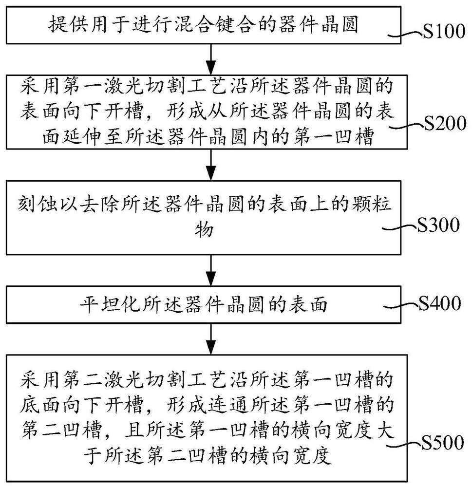
[0039] figure 1 A flow chart of the wafer cutting method provided in this embodiment. like figure 1 As shown, the wafer cutting method includes:

[0040] Step S100: providing a device wafer for hybrid bonding;

[0041] Step S200: using a first laser cutting process to grove downwards along the surface of the device wafer to form a first groove extending from the surface of the device wafer into the device wafer;

[0042] Step S300: etching to remove particles on the surface of the device wafer;

[0043] Step S400: planarizing the surface of the device wafer; and,

[0044] Step S500: Using a second laser cutting process to make grooves downward along the bottom surface of the first groove to form a second groove communicating with the first groove, and the transverse width of the first groove is larger than the first groove Lateral width of the second groove.

[0045] Figure 2a ~ Figure 2f A schematic structural diagram corresponding to corresponding steps of the wafer ...

Embodiment 2

[0070] image 3 A schematic diagram of the cutting lane 200 provided in this embodiment. like image 3 As shown, the difference from Embodiment 1 is that in this embodiment, when the second groove 202 is formed, the second groove 202 penetrates the mixing chamber downward along the bottom of the first groove 201 The bonding layer 120 , the interconnect structure layer 110 and the substrate 100 . In this way, the first groove 201 and the second groove 202 jointly penetrate the device wafer and form the dicing line 200, the step of forming the third groove 203 can be omitted, simplifying the process process.

Embodiment 3

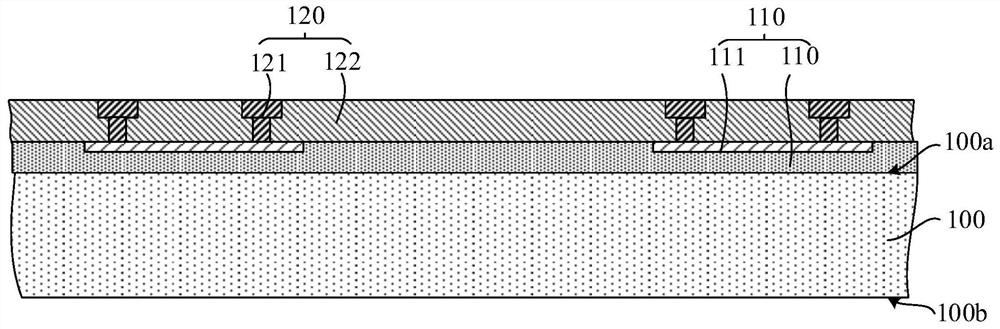
[0072] Figure 4a Schematic diagram of the device wafer provided for this example. like Figure 4a As shown, the difference from Embodiment 1 is that in this embodiment, the device wafer is a device wafer for back-to-face hybrid bonding, and the interconnect structure layer 110 covers the front surface 100a of the substrate 100 , the hybrid bonding layer 120 covers the back surface 100b of the substrate 100 , and the interconnect structure layer 110 has a fourth groove 204 therein.

[0073] Optionally, the fourth groove 204 may be prepared before the hybrid bonding layer 120 of the device wafer is formed, thus, the preparation of the fourth groove 204 will not affect the hybrid bonding The cleanliness and flatness of layer 120 are adversely affected.

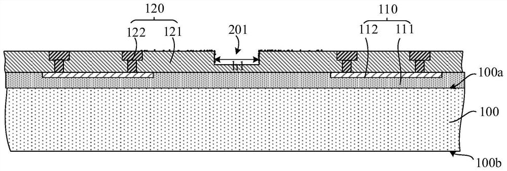
[0074] in particular, Figure 4b A schematic diagram of the cutting lane 200 provided in this embodiment. like Figure 4b As shown, the first groove 201 is located in the hybrid bonding layer 120, the second groove 202 ext...


PUM

PropertyMeasurementUnit
Horizontal widthaaaaaaaaaa
Widthaaaaaaaaaa

Abstract

The invention provides a wafer cutting method. The method comprises the following steps of: firstly, downwards grooving along the surface of a device wafer by adopting a first laser cutting process to form a first groove with larger transverse width, then etching the surface of the device wafer, removing particulate matters which are generated and attached to the surface of the device wafer when the first groove is formed, then flattening the surface of the device wafer, ensuring the cleanliness and flatness of the surface of the device wafer, then adopting a second laser cutting process for grooving downwards along the bottom face of the first groove, and forming a second groove which is communicated with the first groove and is small in transverse width, wherein at the moment, the particles generated by the second laser cutting process are only accumulated in the first groove and the second groove, the cleanliness and flatness of the surface of the device wafer are not affected, the cleanliness and flatness of the surface of a single chip generated after cutting are guaranteed, and the bonding effect of a hybrid bonding process can be improved.

Description

technical field [0001] The invention relates to the technical field of semiconductors, in particular to a wafer cutting method. Background technique [0002] As semiconductor technology enters the post-Moore era, in order to meet the needs of high integration and high performance, the chip structure is developing in a three-dimensional direction. Among them, the realization of "heterogeneous mixing" through bonding technology is one of the important technologies of "Moore's Law". The bonding process can realize high-density interconnection of chips with different process nodes to achieve smaller size and higher performance. and lower power system-level integration. The existing bonding methods usually include wafer-to-wafer bonding (W2W), chip-to-chip bonding (C2C) and chip-to-wafer bonding (C2W). Because C2W can eliminate bad chips and has a high yield, it is favored by global semiconductor giants. [0003] C2W can be realized by pure metal bonding process or hybrid bond...

Claims


Application Information

Patent Timeline
IPC IPC(8): B23K26/38B23K26/402H01L21/78
CPCB23K26/38B23K26/402H01L21/78
Inventor 田应超
Owner HUBEI 3D SEMICON INTEGRATED INNOVATION CENT CO LTD
Why Eureka
Try Eureka