Quaternary-system transparent-substrate-included light-emitting diode and manufacturing method thereof

A technology of light-emitting diodes and transparent substrates, which is applied in the direction of electrical components, circuits, semiconductor devices, etc., can solve problems such as the inability to achieve high light extraction rates, and achieve improved bonding yields, improved light extraction rates, and firm bonding Effect

Active Publication Date: 2018-03-16
YANGZHOU CHANGELIGHT
View PDF3 Cites 5 Cited by
  • Summary
  • Abstract
  • Description
  • Claims
  • Application Information

AI Technical Summary

Problems solved by technology

[0004] In view of this, the present invention provides a quaternary system transparent substrate light-emitting diode and its manufacturing method to solve the problem that the gallium arsenide-based light-emitting diode represented by AlGaInP-LED in the prior art is limited by the material itself and the substrate. Limitations, the problem of not being able to achieve a high light extraction rate

Method used


Image

  • Quaternary-system transparent-substrate-included light-emitting diode and manufacturing method thereof
  • Quaternary-system transparent-substrate-included light-emitting diode and manufacturing method thereof
  • Quaternary-system transparent-substrate-included light-emitting diode and manufacturing method thereof

Examples


example 1

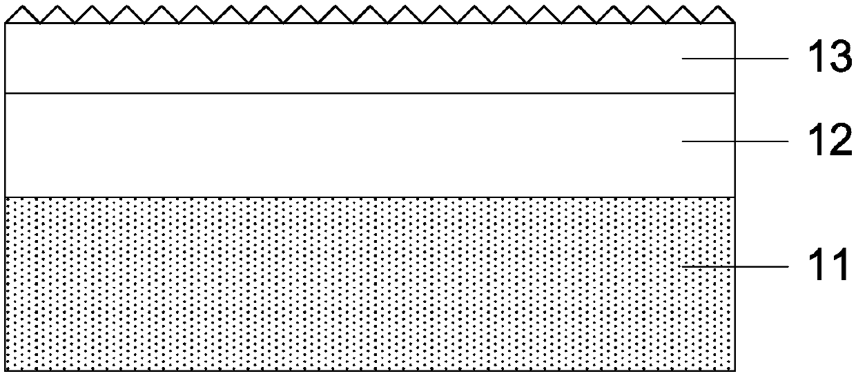
[0084] A method for preparing a quaternary light-emitting diode with a transparent substrate as described above, comprising the steps of:

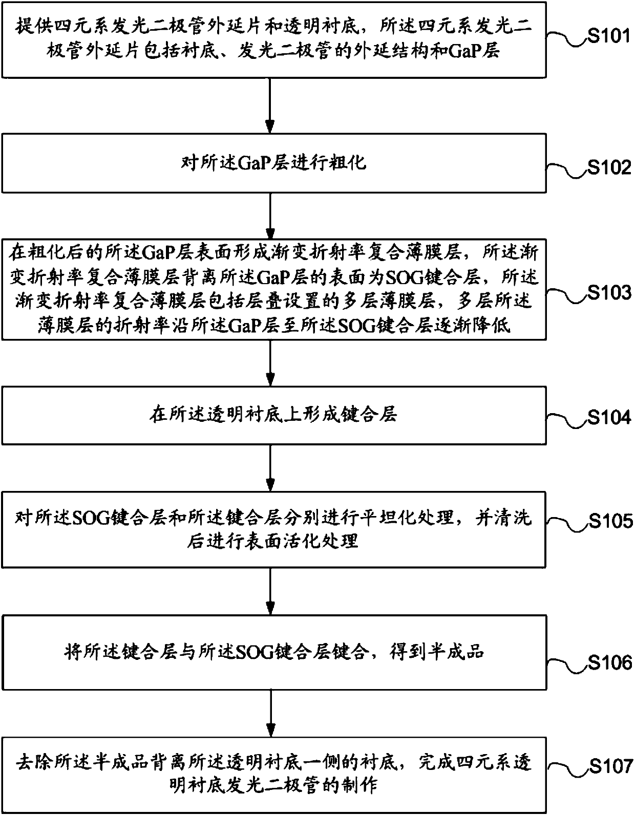
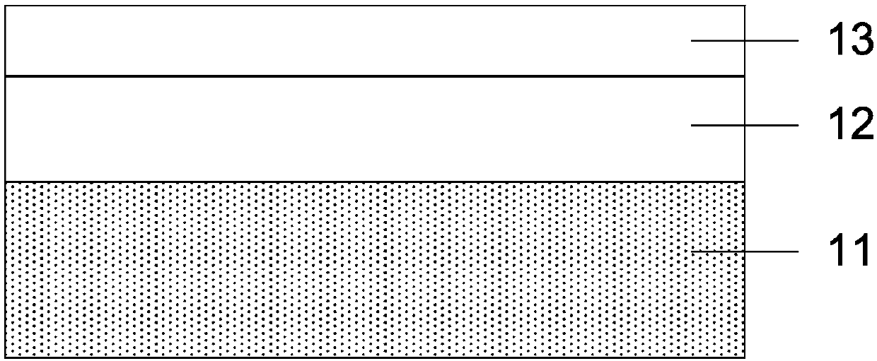
[0085] 1) The surface of the GaP layer of the AlGalnP-LED epitaxial wafer is mechanically ground to obtain a rough surface, which is used as the bonding surface, and then thin films of titanium oxide, zinc oxide, and oxide are deposited on the bonding surface in sequence by electron beams. Aluminum, and then use the method of spin coating, spin coating SOG, wherein, the thickness of SOG is 3um, mainly because the thickness of the polishing layer needs to be thick enough to have a chance to polish flatness; the composite film layer mainly uses the method of gradient refractive index, It is more conducive to the output of light.

[0086] 2) Among them, the surface of the GaP layer is roughened by mechanical grinding;

[0087] 3) Among them, after SOG spin coating, the curing process is carried out according to a certain process. The curing ...

example 2

[0095] A method for preparing a quaternary light-emitting diode with a transparent substrate as described above, comprising the steps of:

[0096] 1) The surface of the GaP layer of the AlGalnP-LED epitaxial wafer is mechanically ground to obtain a roughened surface, which is used as the bonding surface, and then the thin films of titanium oxide and zinc oxide are sequentially deposited on the bonding surface by electron beams, and then Spin-coating is used to spin-coat SOG, and the thickness of SOG is 3um, mainly because the thickness of the polishing layer needs to be thick enough to have a chance to polish flatness; the composite film layer mainly uses the method of refractive index gradient, which is more conducive light output.

[0097] 2) Among them, the surface of the GaP layer is roughened by mechanical grinding;

[0098] 3) Among them, after SOG spin coating, the curing process is carried out according to a certain process. The curing process includes performing on a...

example 3

[0106] A method for preparing a quaternary light-emitting diode with a transparent substrate as described above, comprising the steps of:

[0107] 1) The surface of the GaP layer of the AlGalnP-LED epitaxial wafer is mechanically ground to obtain a roughened surface, which is used as the bonding surface, and then the ITO thin film layer is sequentially deposited on the bonding surface by sputtering, and then spin-coated The method, the spin coating thickness is 3um SOG, mainly because the thickness of the polishing layer needs to be thick enough to have a chance to polish the flatness; the composite thin film layer mainly uses the refractive index gradient method, which is more conducive to the output of light.

[0108] 2) Among them, the surface of the GaP layer is roughened by mechanical grinding;

[0109] 3) Among them, after SOG spin coating, the curing process is carried out according to a certain process. The curing process includes performing on a hot plate. Bake at ℃ ...


PUM


Abstract

The application provides a method for manufacturing a quaternary-system transparent-substrate-included light-emitting diode and a quaternary-system transparent-substrate-included light-emitting diode.On the basis of a transparent substrate bonding technique, a quaternary-system GaAs substrate light-emitting diode epitaxial wafer is transferred to the transparent substrate to replace a substrate made of a light-absorptive material, so that the luminous efficiency is improved. Besides, a GaP layer is roughened and a gradient-refractive-index composite film layer is formed on the GaP layer, so that the light transmittance is enhanced because of the gradient-refractive-index composite film layer and thus the light extraction rate of light-emitting diode is increased. Furthermore, because an SOG bonding layer is arranged at the outermost side of the gradient-refractive-index composite film layer, compared with the prior art with the monox bonding layer, the light-emitting diode has the improved bonding capability; the bonding becomes firm; and the bonding yield is increased.

Description

technical field [0001] The invention relates to the technical field of manufacturing semiconductor devices, in particular to a light-emitting diode with a quaternary system transparent substrate and a manufacturing method thereof. Background technique [0002] Light Emitting Diode (English for Light Emitting Diode, referred to as LED) is a semiconductor light emitting device, which can effectively convert electrical energy into light energy. and other compounds. Most of the white light LEDs currently produced are made by covering a blue light LED (near-UV, wavelength 450nm to 470nm) with a light yellow phosphor coating. White light LEDs are the third generation of electricity after incandescent and fluorescent lamps. The light source has become the goal that light source and lighting research institutions around the world are competing to develop and strive to obtain, and it is a star industry in the future lighting field. [0003] With the mass production of gallium nitri...

Claims


Application Information

Patent Timeline
Patent Type & Authority Applications(China)
IPC IPC(8): H01L33/30H01L33/26H01L33/00
CPCH01L33/0062H01L33/26H01L33/30
Inventor 李波杨凯邹微微徐洲张双翔
Owner YANGZHOU CHANGELIGHT
Why Eureka
Try Eureka