Monolithic ceramic electronic component and mounting structure thereof

a technology of ceramic electronic components and monolithic ceramics, applied in the direction of fixed capacitor details, stacked capacitors, fixed capacitors, etc., can solve the problems of high point of pb-free solder, high cost, and high cost of ceramic electronic components, and achieves high precision, easy formation, and high production efficiency.

Active Publication Date: 2010-04-15
MURATA MFG CO LTD
View PDF11 Cites 31 Cited by
  • Summary
  • Abstract
  • Description
  • Claims
  • Application Information

AI Technical Summary

Benefits of technology

[0016]The squeezing out of the electrically conductive adhesive in the lateral direction and the contact of the electrically conductive adhesive with the lower surface of the ceramic element assembly occur readily as the size of the monolithic ceramic electronic component is reduced. This is because when the dimensions of the monolithic ceramic electronic component are relatively large, the radii of curvature of corner portions and ridge portions of the ceramic element assembly increase, the region into which the electrically conductive adhesive runs away is extended, and the electrically conductive adhesive does not readily reach the lower surface of the ceramic element assembly. On the other hand, it is believed that when the dimension of the monolithic ceramic electronic component is reduced, the size of the region into which the electrically conductive adhesive runs away is reduced and, therefore, the lower surface of the ceramic element assembly is reached more easily.
[0040]In the mounting structure of the monolithic ceramic electronic component according to various preferred embodiments of the present invention, mounting is performed on the mounting substrate from the side of the first side surface of the ceramic element assembly using the electrically conductive adhesive such that the directions of the first and the second internal electrodes become perpendicular or substantially perpendicular to the mounting substrate. Therefore, the second electrically conductive adhesive connecting the second external terminal electrode and the second land does not extend under the end point, which is closest to the first side surface and which is closest to the second end surface, in the first region of the first internal electrode. Consequently, the field strength between the second electrically conductive adhesive and the first internal electrode can be reduced. Thus, migration due to a metal filler in the electrically conductive adhesive can be effectively prevented. As a result, the electrical characteristics of a monolithic ceramic electronic component does not readily deteriorate after mounting is performed using the electrically conductive adhesive. Then, the mounting structure of a monolithic ceramic electronic component exhibiting excellent reliability and having stable characteristics can be provided.

Problems solved by technology

However, the melting point of the Pb-free solder is relatively high and, therefore, a treatment at high temperatures is required during soldering.
As a result, cracking often occurs in a ceramic element assembly of the ceramic electronic component because of a difference in the thermal expansion coefficient between the ceramic element assembly and an external terminal electrode.
However, in the case in which a ceramic electronic component was mounted on a substrate using an electrically conductive adhesive, in practice, the characteristics of the ceramic electronic component are likely to be deteriorated.
That is, even when the characteristics were measured at a ceramic electronic component stage and it was determined that the characteristics were good, when evaluation was performed after the ceramic electronic component was mounted using the electrically conductive adhesive, the characteristics deteriorated in some instances.
However, Japanese Unexamined Patent Application Publication No. 9-50935 does not recognize or identify a problem when the monolithic ceramic electronic component is mounted using an electrically conductive adhesive.

Method used


Image

  • Monolithic ceramic electronic component and mounting structure thereof
  • Monolithic ceramic electronic component and mounting structure thereof
  • Monolithic ceramic electronic component and mounting structure thereof

Examples


Embodiment Construction

[0055]The specific preferred embodiments according to the present invention will be described below with reference to drawings.

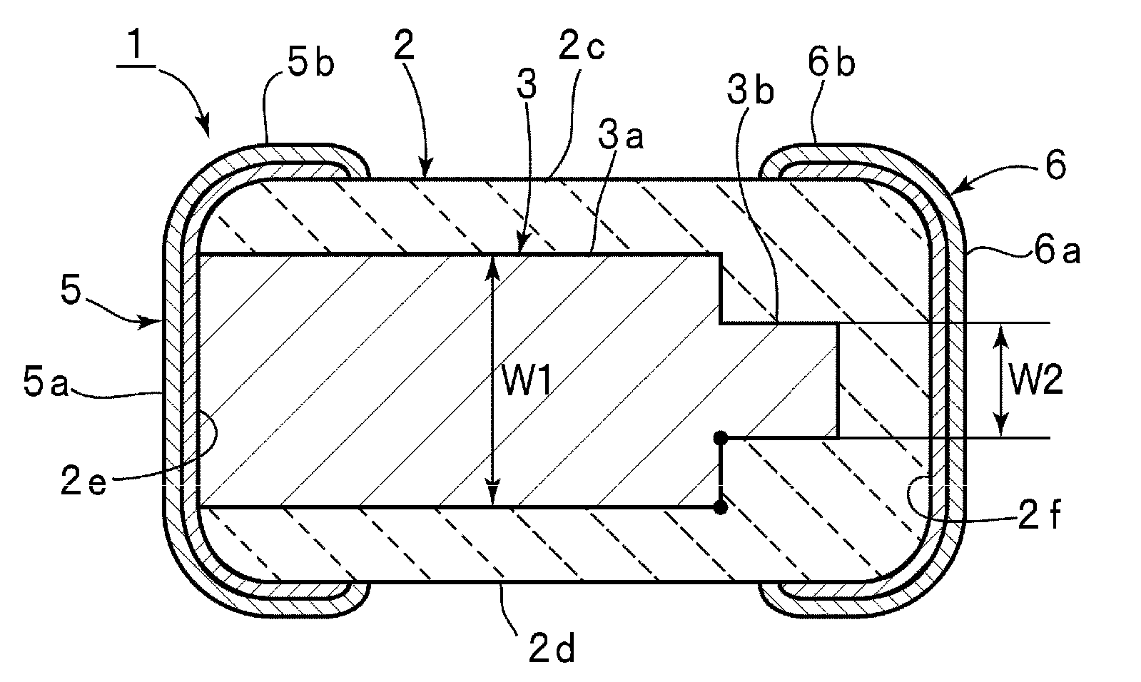
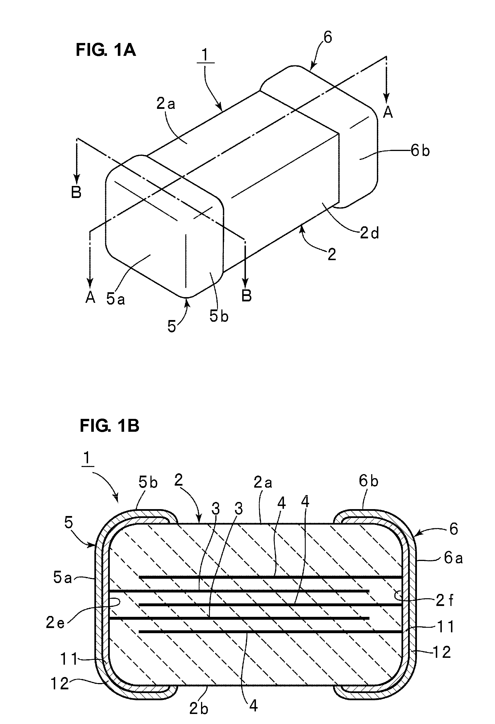
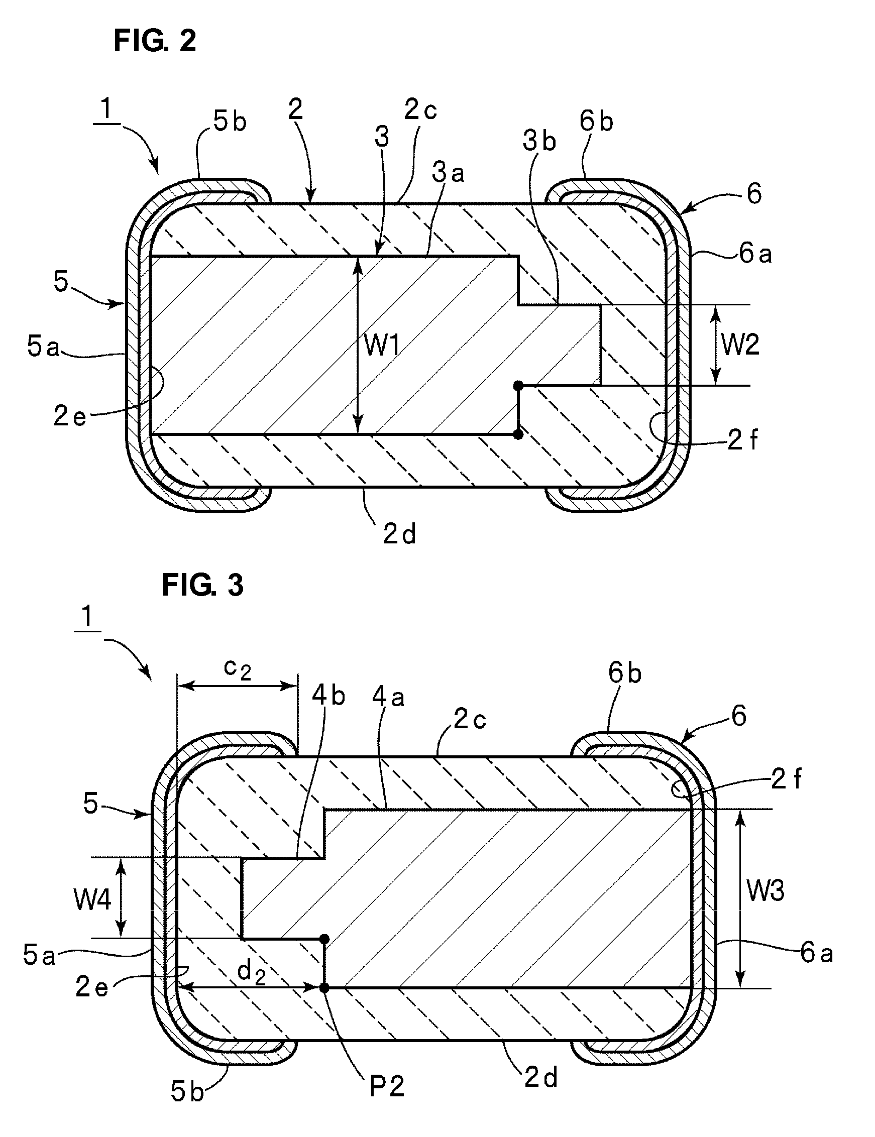
[0056]FIG. 1A is a perspective view of a monolithic ceramic electronic component according to a first preferred embodiment of the present invention, and FIG. 1B is a sectional front view of the section taken along a line A-A shown in FIG. 1A.

[0057]A monolithic ceramic electronic component 1 according to the present preferred embodiment is a monolithic ceramic capacitor, for example.

[0058]The ceramic electronic component 1 includes a ceramic element assembly 2 formed by laminating a plurality of ceramic layers. The ceramic material defining the ceramic element assembly 2 is not specifically limited, and an appropriate dielectric ceramic can be used. In the present preferred embodiment, BaTiO3 based ceramic is preferably used, for example.

[0059]The ceramic element assembly 2 has first and second principal surfaces 2a and 2b, which preferably have a substantial...


PUM

PropertyMeasurementUnit
temperatureaaaaaaaaaa
dimensionaaaaaaaaaa
widthaaaaaaaaaa

Abstract

A monolithic ceramic electronic component includes a first internal electrode including a first region which extends to a first end surface and which has a relatively large dimension in a width direction and a second region which is located at the side closer to a front end than is the first region and which has a relatively small dimension in a width direction, wherein d1>c1+ng (n represents a constant determined in accordance with the size of the monolithic ceramic electronic component) is satisfied, where the distance from a first end point which is closest in the first region to the first side surface and which is closest to the second end surface to the second end surface is d1, the distance between first and second wraparound portions and is g, and the distance between a front end of the second wraparound portion and the second end surface is c1 while a first side surface defines a mounting surface.

Description

BACKGROUND OF THE INVENTION[0001]1. Field of the Invention[0002]The present invention relates to a monolithic ceramic electronic component, e.g., a monolithic capacitor, and a mounting structure thereof. In particular, the present invention relates to a monolithic ceramic electronic component, which is mounted with an electrically conductive adhesive, and a mounting structure thereof.[0003]2. Description of the Related Art[0004]Recently, in order to reduce the environmental load, Pb-free solder including no Pb has been used to mount a monolithic ceramic electronic component. However, the melting point of the Pb-free solder is relatively high and, therefore, a treatment at high temperatures is required during soldering. As a result, cracking often occurs in a ceramic element assembly of the ceramic electronic component because of a difference in the thermal expansion coefficient between the ceramic element assembly and an external terminal electrode.[0005]In addition, an electrically...

Claims


Application Information

Patent Timeline
Patent Type & Authority Applications(United States)
IPC IPC(8): H01G4/12
CPCH01G4/012H01G4/30H01G4/232
Inventor KOGA, SEIJISANADA, YUKIO
Owner MURATA MFG CO LTD
Why Eureka
Try Eureka