Thin-film piezoelectric device, production method thereof, head gimbals assembly using the thin-film piezoelectric device, and hard disk drive using the head gimbals assembly

a thin-film piezoelectric device and piezoelectric technology, applied in the direction of piezoelectric/electrostrictive device details, device material selection, instruments, etc., can solve the problems of single-layer piezoelectric laminate structure failing to achieve higher performance and reliability of thin-film piezoelectric device, and achieves higher reliability and high performance. the effect of high efficiency and lower cost of the apparatus

Active Publication Date: 2010-04-22
TDK CORPARATION +1
View PDF13 Cites 10 Cited by
  • Summary
  • Abstract
  • Description
  • Claims
  • Application Information

AI Technical Summary

Benefits of technology

[0011]In the production method of the thin-film piezoelectric device, therefore, various stresses generated between the piezoelectric layer and the first substrate due to heat, crystal lattice constant mismatch, etc. in the first laminate forming step are released by removal of the first substrate in the first substrate removing step and the various stresses thus released are transferred to the second substrate. At this time, since the adhesive layer of the material with the Young's modulus smaller than that of the piezoelectric layer is interposed between the piezoelectric layer and the second substrate, the various stresses to be transferred to the second substrate are relaxed by the adhesive layer. For this reason, the warpage and flexural displacement of the device is effectively suppressed even though the thin-film piezoelectric device obtained by the production method of the present invention consists of the single-layer piezoelectric laminate. Since the device of the present invention adopts the structure in which the adhesive layer is sandwiched between the second electrode layer and the support layer and in which the respective Young's moduli of the second electrode layer and the support layer are larger than the Young's modulus of the adhesive layer, the warpage and flexural displacement of the device is more suppressed. Since the device consists of the single-layer piezoelectric laminate, the production cost thereof is reduced. Therefore, the production method of the thin-film piezoelectric device according to the present invention permits us to readily produce the thin-film piezoelectric device capable of achieving higher performance, higher reliability, and lower cost by the single-layer piezoelectric laminate.
[0020]The present invention provides the thin-film piezoelectric device capable of achieving higher performance, higher reliability and lower cost by the single-layer piezoelectric laminate, the production method thereof, and the head gimbals assembly using the thin-film piezoelectric device.

Problems solved by technology

However, all the thin-film piezoelectric devices disclosed in Patent Literatures 1-3 have the two piezoelectric laminates including the respective piezoelectric layers and this configuration makes it difficult to satisfy the market demands of mass productivity and low price.
For this reason, a single-layered piezoelectric laminate structure failed to achieve higher performance and higher reliability of the thin-film piezoelectric device and an apparatus incorporating the thin-film piezoelectric device of this structure inevitably suffered breakage, trouble, and so on.

Method used


Image

  • Thin-film piezoelectric device, production method thereof, head gimbals assembly using the thin-film piezoelectric device, and hard disk drive using the head gimbals assembly
  • Thin-film piezoelectric device, production method thereof, head gimbals assembly using the thin-film piezoelectric device, and hard disk drive using the head gimbals assembly
  • Thin-film piezoelectric device, production method thereof, head gimbals assembly using the thin-film piezoelectric device, and hard disk drive using the head gimbals assembly

Examples


Embodiment Construction

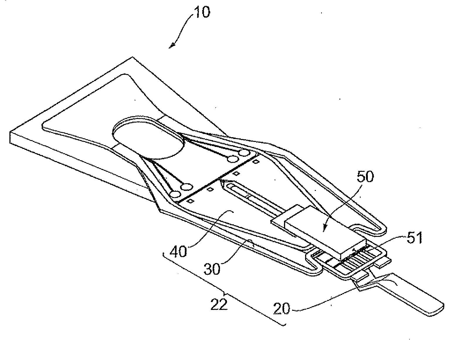
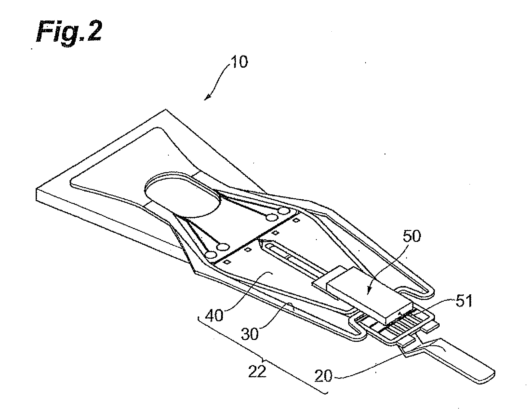
[0032]The preferred embodiment of thin-film piezo actuator (thin-film piezoelectric device) 40 and Head Gimbals Assembly (HGA) 10 according to the present invention will be described below in detail with reference to the accompanying drawings. In the description of the drawings the same elements will be denoted by the same reference symbols, without redundant description.

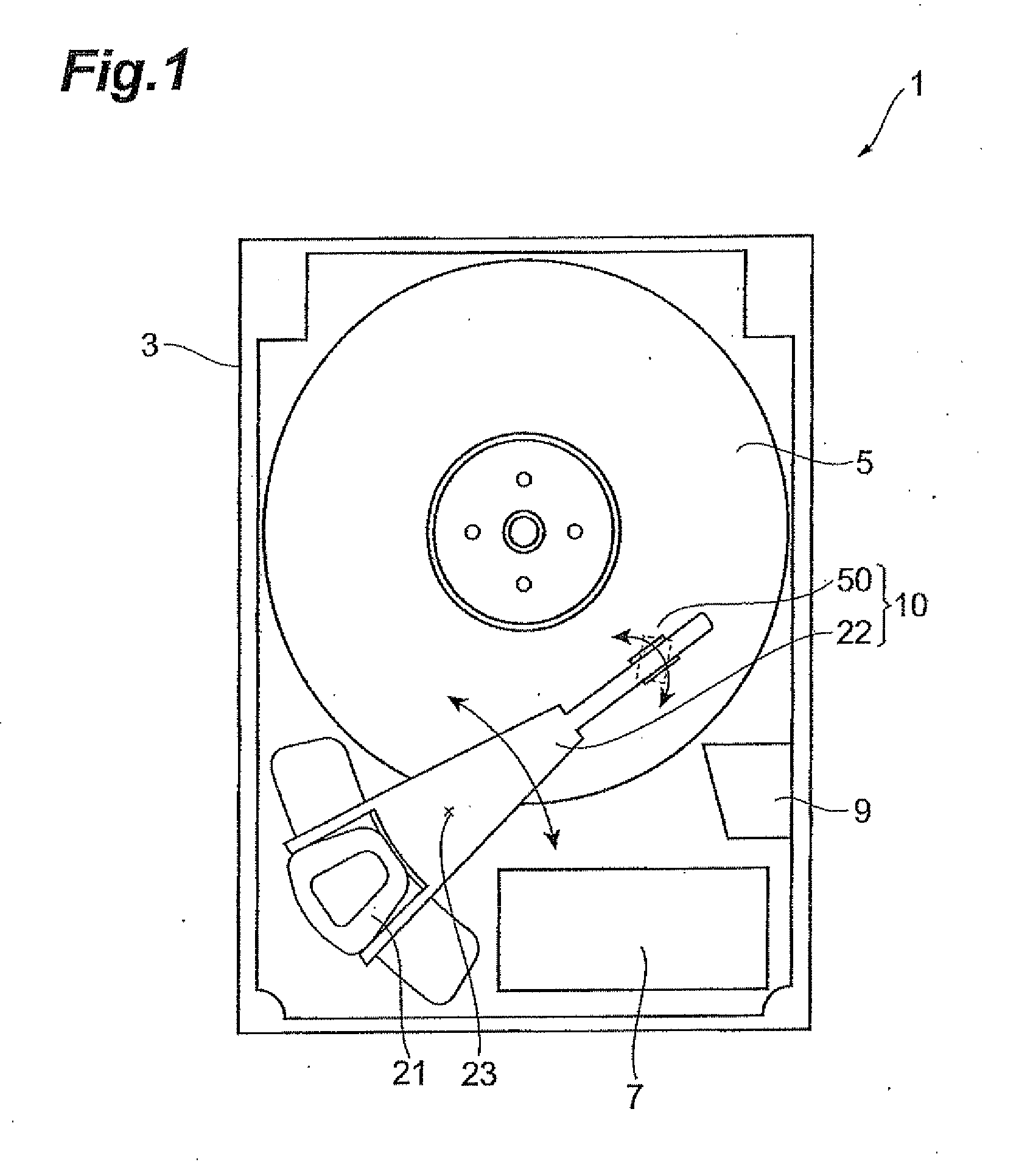
[0033]First, prior to the description of the thin-film piezo actuator 40 and HGA 10 according to the embodiment, an example of hard disk device (hard disk drive) 1 to which they are applied will be described. FIG. 1 is a drawing showing the hard disk device 1 equipped with HGA 10 according to the present embodiment. The hard disk device 1 is a device that actuates HGA 10 to record and reproduce magnetic information in and from a recording surface of hard disk 5 under high-speed rotation by thin-film magnetic head 51 of head slider 50.

[0034]The hard disk device 1 comprises the hard disk 5 as a recording medium, HGA 1...


PUM

PropertyMeasurementUnit
Young's modulusaaaaaaaaaa
thickness t1aaaaaaaaaa
Young's modulusaaaaaaaaaa

Abstract

A method includes a step of stacking a first electrode layer, a piezoelectric layer, and a second electrode layer on a first substrate to form a first laminate; a step of stacking a support layer on a second substrate to form a second laminate; a step of bonding the first and second laminates through an adhesive layer to form a third laminate; a step of removing the first substrate from the third laminate; a step of processing the third laminate in a desired shape; and a step of removing the second substrate. A Young's modulus of the adhesive layer is smaller than a Young's modulus of the piezoelectric layer. Respective Young's moduli of the second electrode layer and the support layer are larger than the Young's modulus of the adhesive layer. The third laminate has no other piezoelectric layer except for the aforementioned piezoelectric layer.

Description

BACKGROUND OF THE INVENTION[0001]1. Field of the Invention[0002]The present invention relates to a thin-film piezoelectric device used for fine positioning by inverse piezoelectric effect of piezoelectric layer, a production method thereof, and a head gimbals assembly using the thin-film piezoelectric device and, more particularly, to a positioning structure for a magnetic head which performs reading and writing of recording information in a magnetic recording disk device.[0003]2. Related Background Art[0004]The recent approach toward higher density and larger capacity of magnetic recording (hard disk) increases the necessity for a thin-film piezoelectric device as a high-accuracy positioning mechanism of tracking. For example, Patent Literatures 1-3 below disclose the thin-film piezoelectric devices of this kind.[0005]Patent Literature 1 (Japanese Patent Application Laid-open No. 2005-286037) discloses the thin-film piezoelectric device in which a piezoelectric laminate 21A wherein...

Claims


Application Information

Patent Timeline
Patent Type & Authority Applications(United States)
IPC IPC(8): G11B5/48H01L41/22H01L41/04G11B21/10G11B21/21H01L41/09H01L41/18H01L41/23H01L41/313
CPCG11B5/4826G11B5/4873G11B5/5552G11B5/596Y10T29/42H01L41/1876H01L41/316H01L41/319H01L41/0986G11B5/4833H10N30/206H10N30/8554H10N30/079H10N30/076
Inventor HATA, KENJIROSASAKI, HIROFUMIKURACHI, KATSUYUKI
Owner TDK CORPARATION
Why Eureka
Try Eureka