Photovoltaic device and method for manufacturing the same

a technology of photovoltaic devices and manufacturing methods, applied in semiconductor devices, pv power plants, coatings, etc., can solve problems such as pattern deterioration, reduce the number of laser scribes, improve the interface characteristic of solar cells, and reduce the manufacturing cost of solar cells

Inactive Publication Date: 2010-04-29
SAMSUNG DISPLAY CO LTD +1
View PDF8 Cites 57 Cited by
  • Summary
  • Abstract
  • Description
  • Claims
  • Application Information

AI Technical Summary

Benefits of technology

[0052]According to the present invention, the number of laser scribes may be reduced, thereby reducing the manufacturing cost of the solar cell and improving the interface characteristic of the solar cell, and as a result the efficiency of the photovoltaic device may be increased.
[0053]Also, light absorption layers between the neighboring cells are connected thereby improving photo-efficiency, and the light absorption layers are filled in the separation spaces between the neighboring cells such that impurity adhesion or chemical contamination that may be generated during the process is prevented, thereby suppressing a leakage current of the side surface thereof. Also, the connection electrode between the cells is not floated on the light absorption layer, but contacts the light absorption layer such that mechanical durability of the connection electrode may be improved.

Problems solved by technology

However, when the PIN layer is formed in the vertical direction, several laser patternings are executed to the cells when connecting the electrodes of the P layer and the N layer of different cells such that layer damage may be generated and a remaining layer is generated on the side, thereby generating pattern deterioration.

Method used


Image

  • Photovoltaic device and method for manufacturing the same
  • Photovoltaic device and method for manufacturing the same
  • Photovoltaic device and method for manufacturing the same

Examples


Embodiment Construction

[0063]The present invention will be described more fully hereinafter with reference to the accompanying drawings, in which embodiments of the invention are shown. However, the present invention is not limited to embodiments described herein, and may be embodied in other forms. Rather, embodiments described herein are provided to thoroughly and completely understand the disclosed contents and to sufficiently transfer the ideas of the present invention to a person of ordinary skill in the art.

[0064]In the drawings, the thicknesses of layers and regions are exaggerated for clarity. It is to be noted that when a layer is referred to as being “on” another layer or substrate, it can be directly formed on the other layer or substrate or can be formed on the other layer or substrate with a third layer interposed therebetween. Like constituent elements are denoted by like reference numerals throughout the specification.

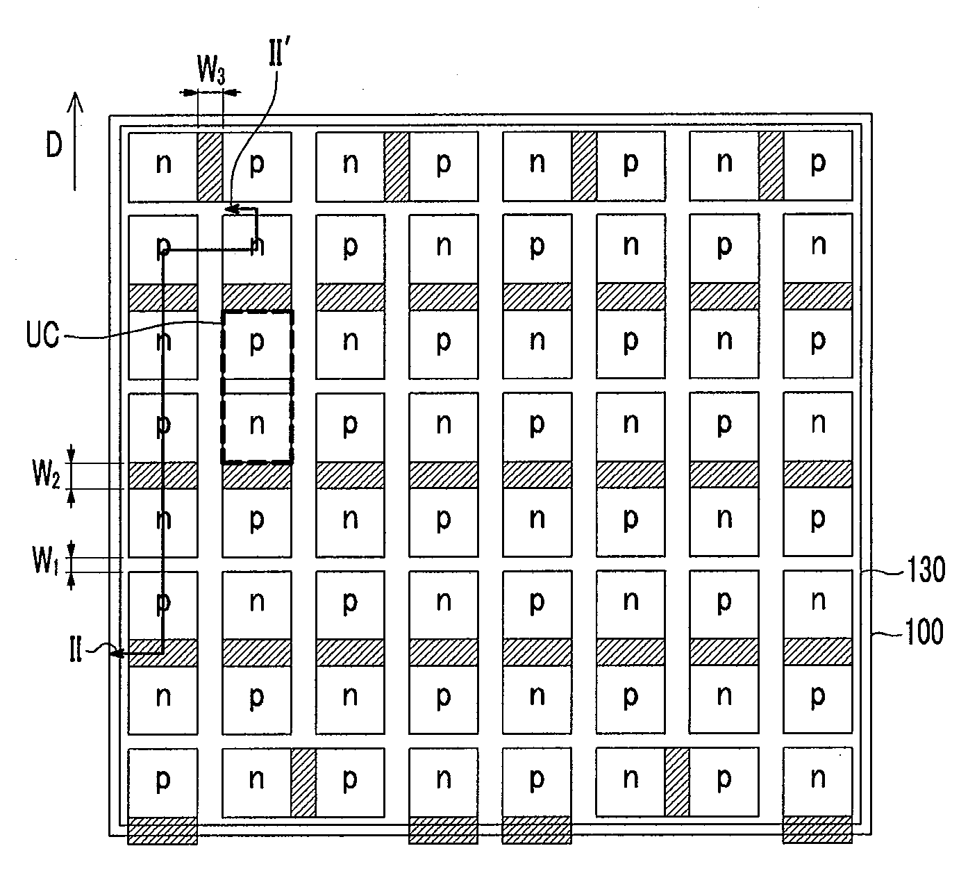
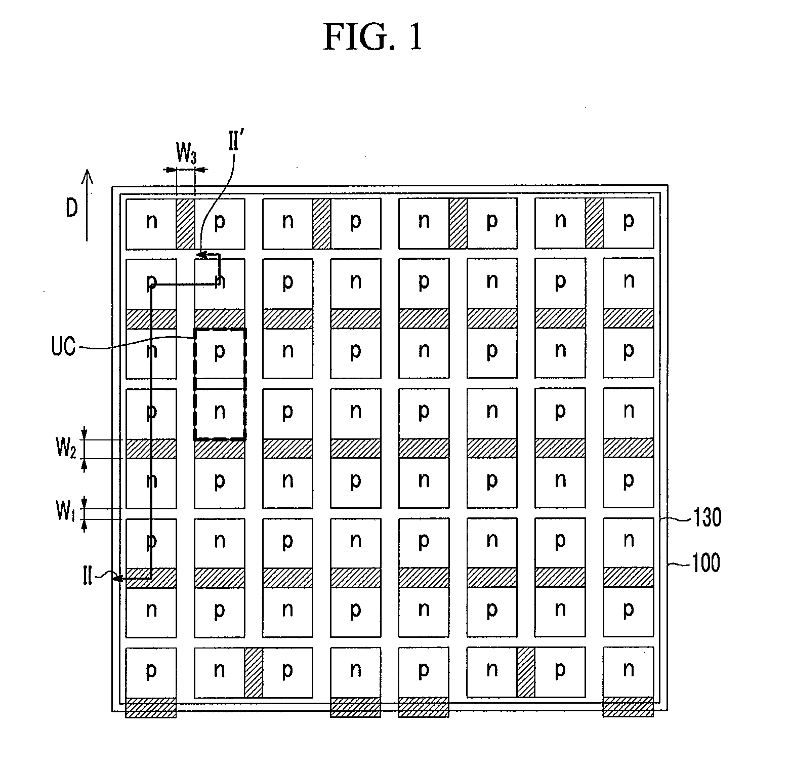
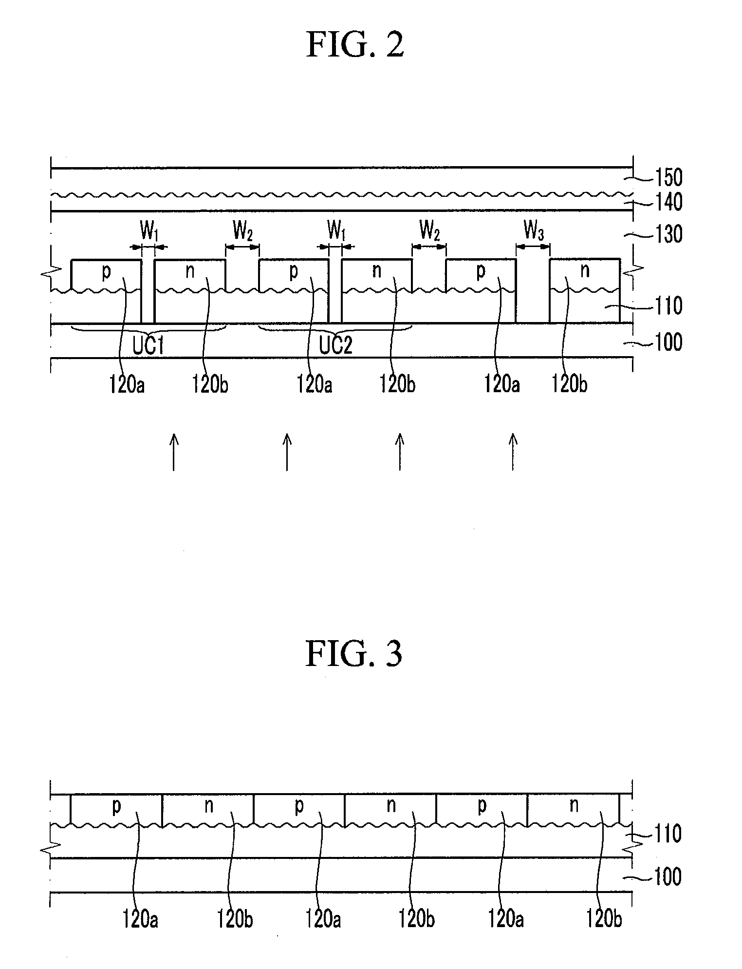
[0065]FIG. 1 is a top plan view of a solar cell according to an embodimen...


PUM

PropertyMeasurementUnit
sizeaaaaaaaaaa
unit cellsaaaaaaaaaa
conductiveaaaaaaaaaa

Abstract

A photovoltaic device and a manufacturing method thereof are provided. The photovoltaic device includes: a substrate; a first conductive layer formed on the substrate; P layers and N layers alternately formed along a first direction on the first conductive layer; and I layers covering the P layers and the N layers on the first conductive layer, wherein the P layers and the N layers are separated from each other by a first interval, the I layers are formed between the P layers and the N layers that are separated by the first interval, and the P layers, the I layers, and the N layers formed along the first direction form unit cells.

Description

CROSS-REFERENCE TO RELATED APPLICATION[0001]This application claims priority to and the benefit of Korean Patent Application No. 10-2008-0104295 filed in the Korean Intellectual Property Office on Oct. 23, 2008 and Korean Patent Application No. 10-2008-0110615 filed in the Korean Intellectual Property Office on Nov. 7, 2008, the entire contents of which are incorporated herein by reference.BACKGROUND OF THE INVENTION[0002](a) Field of the Invention[0003]The present invention relates to a photovoltaic device and a manufacturing method thereof.[0004](b) Description of the Related Art[0005]A solar cell is one kind of photovoltaic device for converting light energy into electrical energy, and is used as a core element for developing solar light. The solar cell is a diode consisting of a PN junction, and may be classified into various kinds according to the material used as a light absorption layer.[0006]A solar cell using silicon as the light absorption layer may be classified as a crys...

Claims


Application Information

Patent Timeline
Patent Type & Authority Applications(United States)
IPC IPC(8): H01L31/042H01L31/04H01L31/05H01L31/20H01L31/18H01L21/283H01L31/075
CPCH01L31/022425H01L31/046Y02E10/548H01L31/075H01L31/022441
Inventor PARK, MINOH, MIN-SEOKKIM, JUNG-TAELEE, CZANG-HOSHIN, MYUNG-HUNLEE, BYOUNG-KYUKANG, KU-HYUNNAM, YUK-HYUNJUNG, SEUNG-JAELIM, MI-HWASEO, JOON-YOUNG
Owner SAMSUNG DISPLAY CO LTD
Why Eureka
Try Eureka