

Semiconductor device
- Summary
- Abstract
- Description
- Claims
- Application Information
AI Technical Summary
Benefits of technology
Problems solved by technology
Method used
Image

Examples
first embodiment
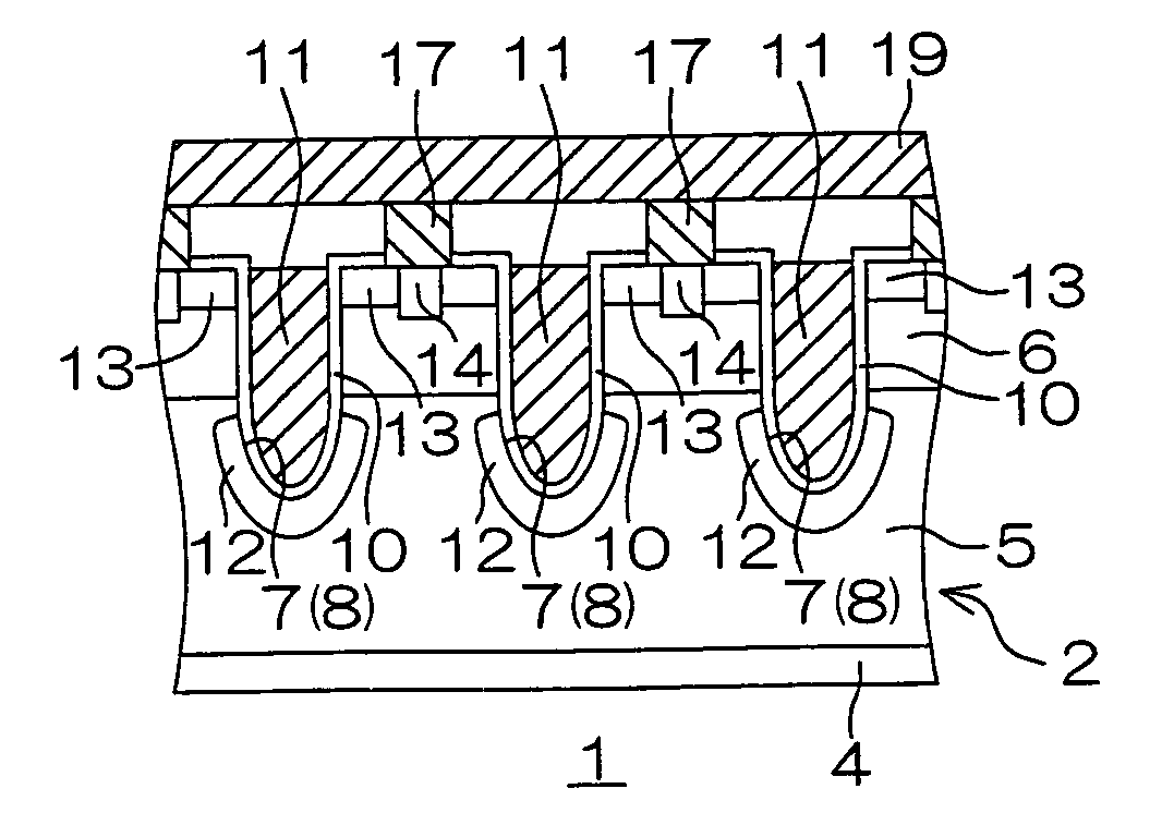
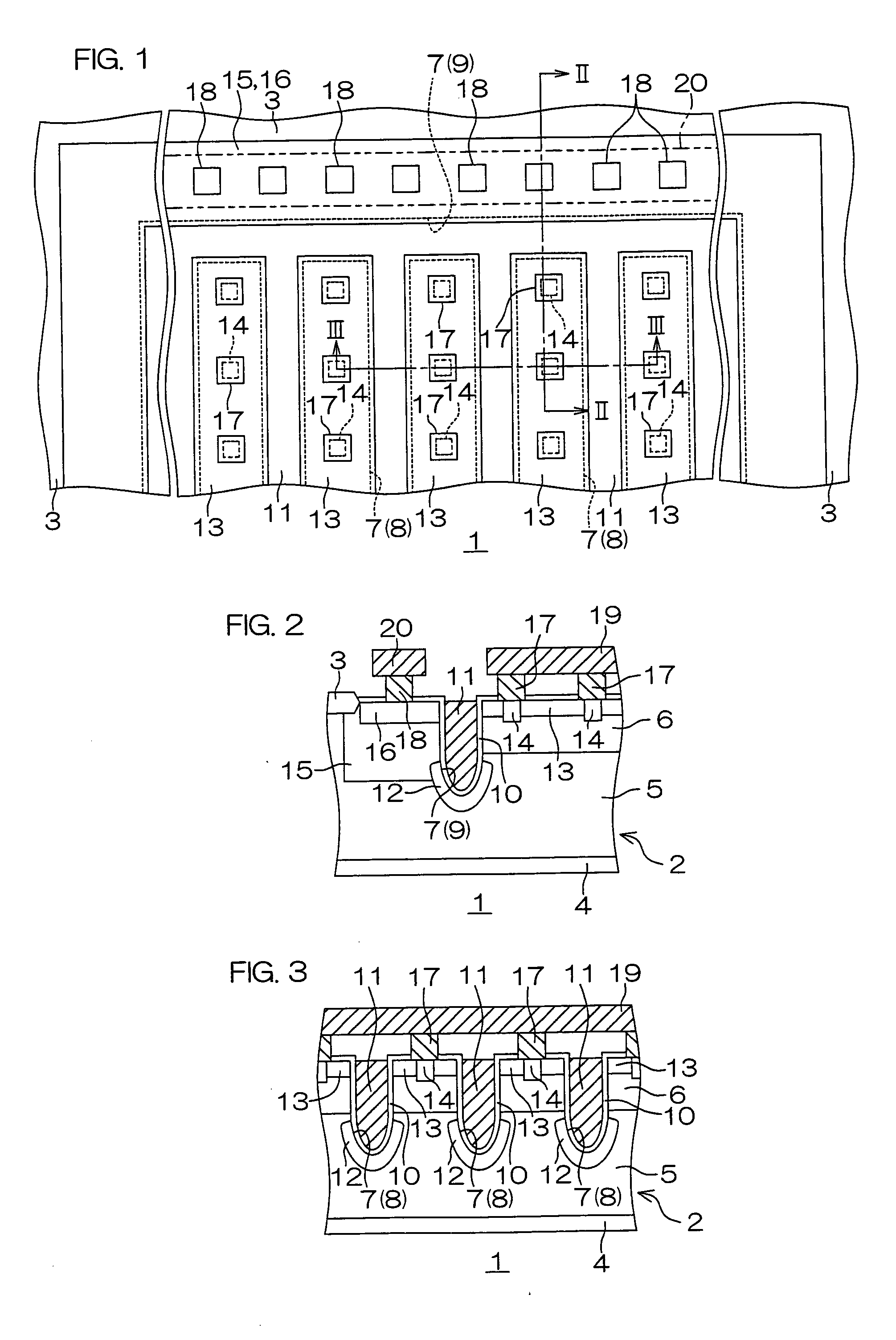
[0038]FIG. 1 is a schematic plan view of a semiconductor device according to the present invention. FIG. 2 is a sectional view of the semiconductor device taken along a section line II-II in FIG. 1. FIG. 3 is a sectional view of the semiconductor device taken along a section line III-III in FIG. 1.
[0039]As shown in FIGS. 2 and 3, the semiconductor device 1 includes a semiconductor layer 2. The semiconductor layer 2 is composed of, for example, silicon. As shown in FIG. 1, a looped field oxide film (e.g., a silicon oxide film formed by a LOCOS (local-oxidation-of-silicon) method) 3 is provided in a surface of the semiconductor layer 2. The field oxide film 3 isolates a region surrounded by the field oxide film 3 from a region outside the field oxide film 3. A plurality of VDMOSs connected in parallel are provided in the region surrounded by the field oxide film 3.
[0040]As shown in FIGS. 2 and 3, the semiconductor layer 2 includes an N++-type drain region 4 (having a higher N-type imp...
second embodiment
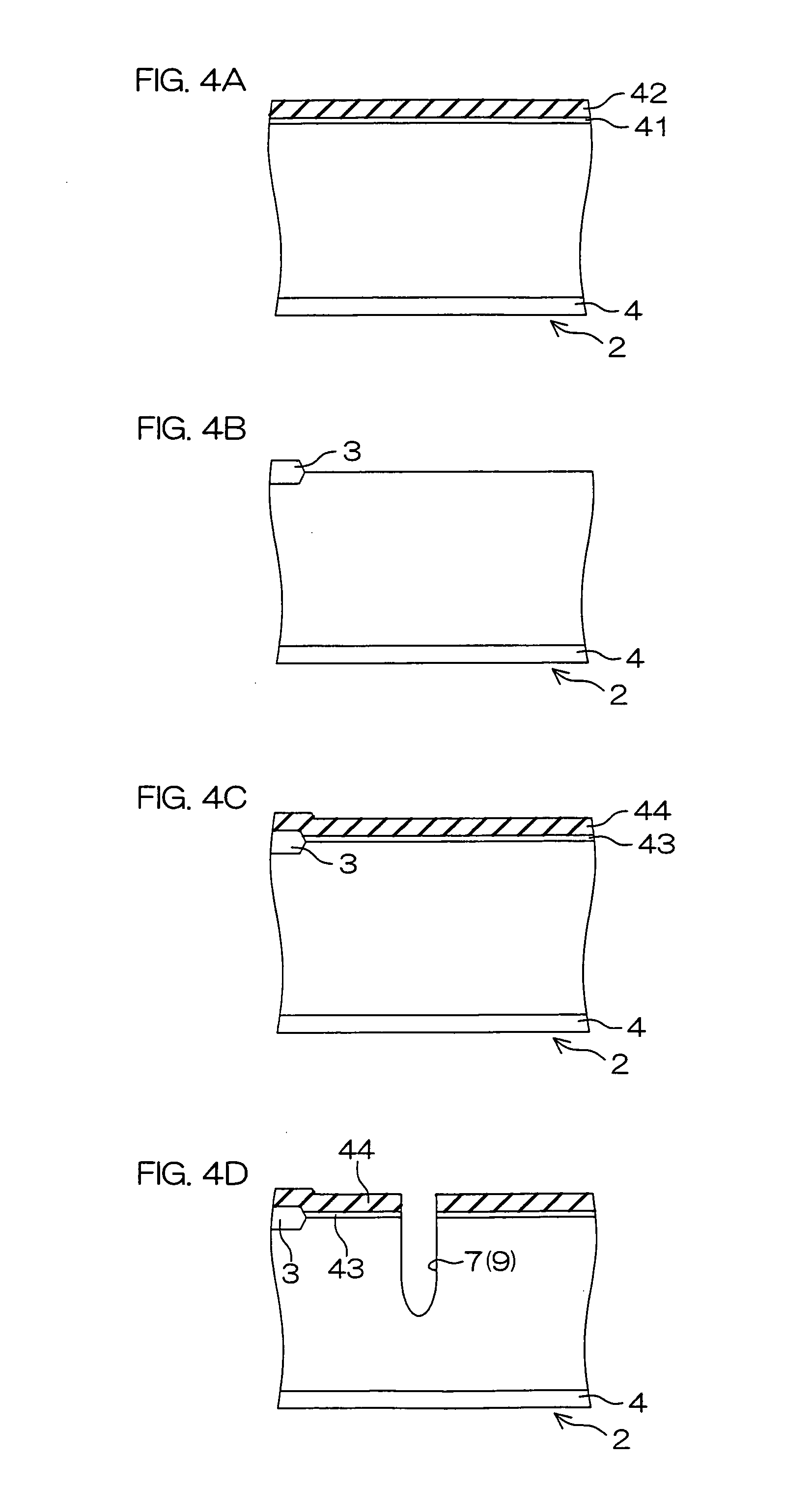
[0068]FIG. 6 is a schematic sectional view showing the construction of a semiconductor device according to the present invention. In FIG. 6, components corresponding to those shown in FIG. 2 are denoted by the same reference characters as in FIG. 2. Further, the semiconductor device shown in FIG. 6 has the same plan view as the semiconductor device shown in FIG. 2, i.e., the same plan view as shown in FIG. 1. FIG. 6 is taken along the same sectional plane as shown FIG. 2. Hereinafter, only differences in construction between the semiconductor device shown in FIG. 6 and the semiconductor device shown in FIG. 2 will be described, and no description will be given to components denoted by the same reference characters.
[0069]In the semiconductor device 61 shown in FIG. 6, the second impurity region 15 has the same depth as the body region 6. A buried impurity region 62 of P-type is provided below the second impurity region 15. The buried impurity region 62 is connected to the second impu...
PUM
 Abstract
Description
Claims
Application Information