Method for manufacturing a semiconductor device having a heat spreader

Inactive Publication Date: 2010-04-29
RENESAS ELECTRONICS CORP
View PDF7 Cites 1 Cited by
  • Summary
  • Abstract
  • Description
  • Claims
  • Application Information

AI Technical Summary

Benefits of technology

[0013]On the other hand, according to the present invention, in the shaving the resin sealing body (10) from the side of the wiring board (S52), at least part of the resin sealing body (10) is shaved from the side of the wiring board (1) in the direction of the thickness of the resin sealing body (10). Consequently, when shaving the resin sealing body (10) from the side of the heat spreader (5), it is jus

Problems solved by technology

And because the bur has conductivity, the semiconductor device, if it is mounted on a board while a bur or a fragment of a pealed b

Method used


Image

  • Method for manufacturing a semiconductor device having a heat spreader
  • Method for manufacturing a semiconductor device having a heat spreader
  • Method for manufacturing a semiconductor device having a heat spreader

Examples


Example

[0057]Hereunder, there will be described the first embodiment of the present invention with reference to the accompanying drawings.

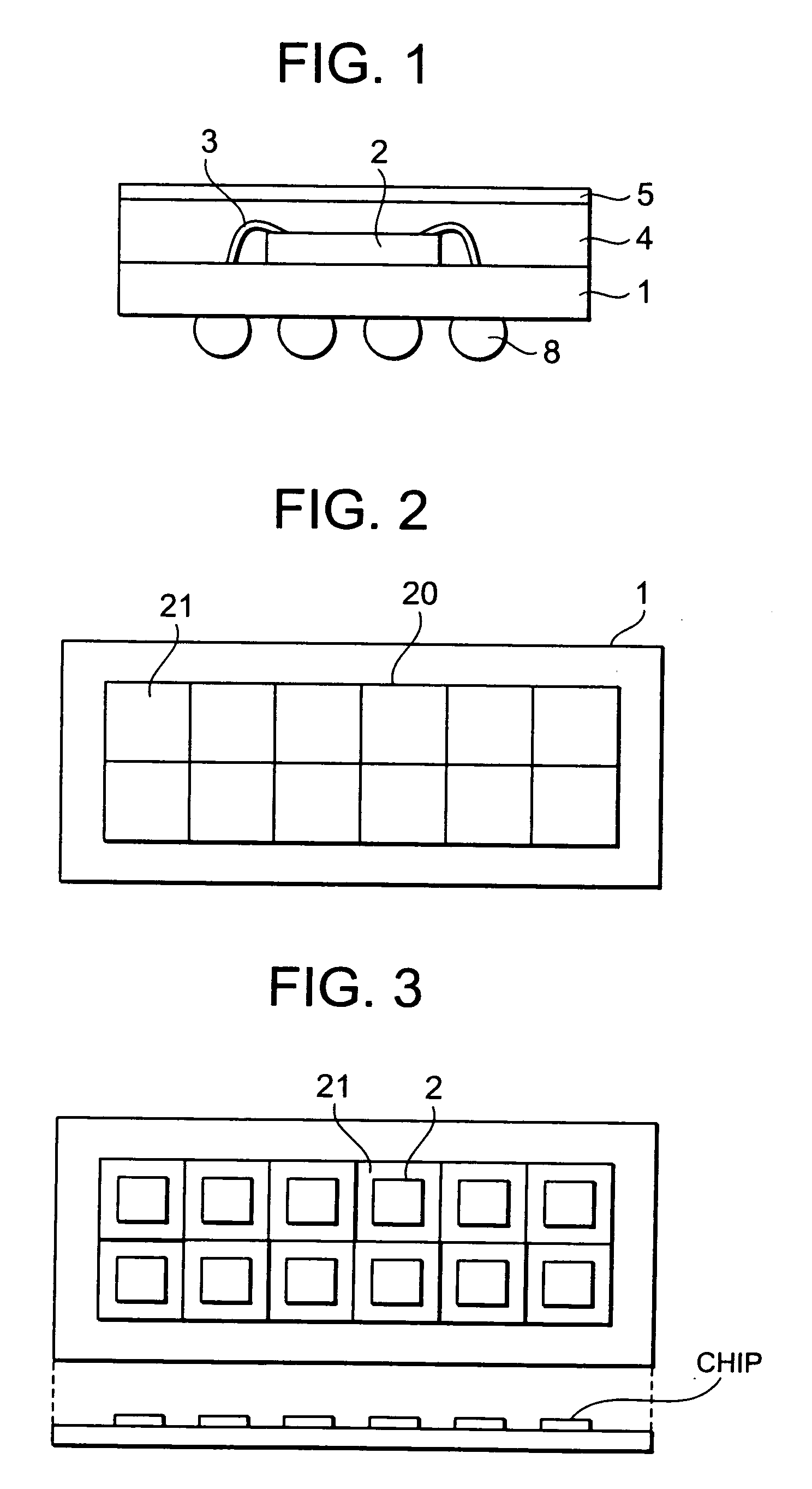
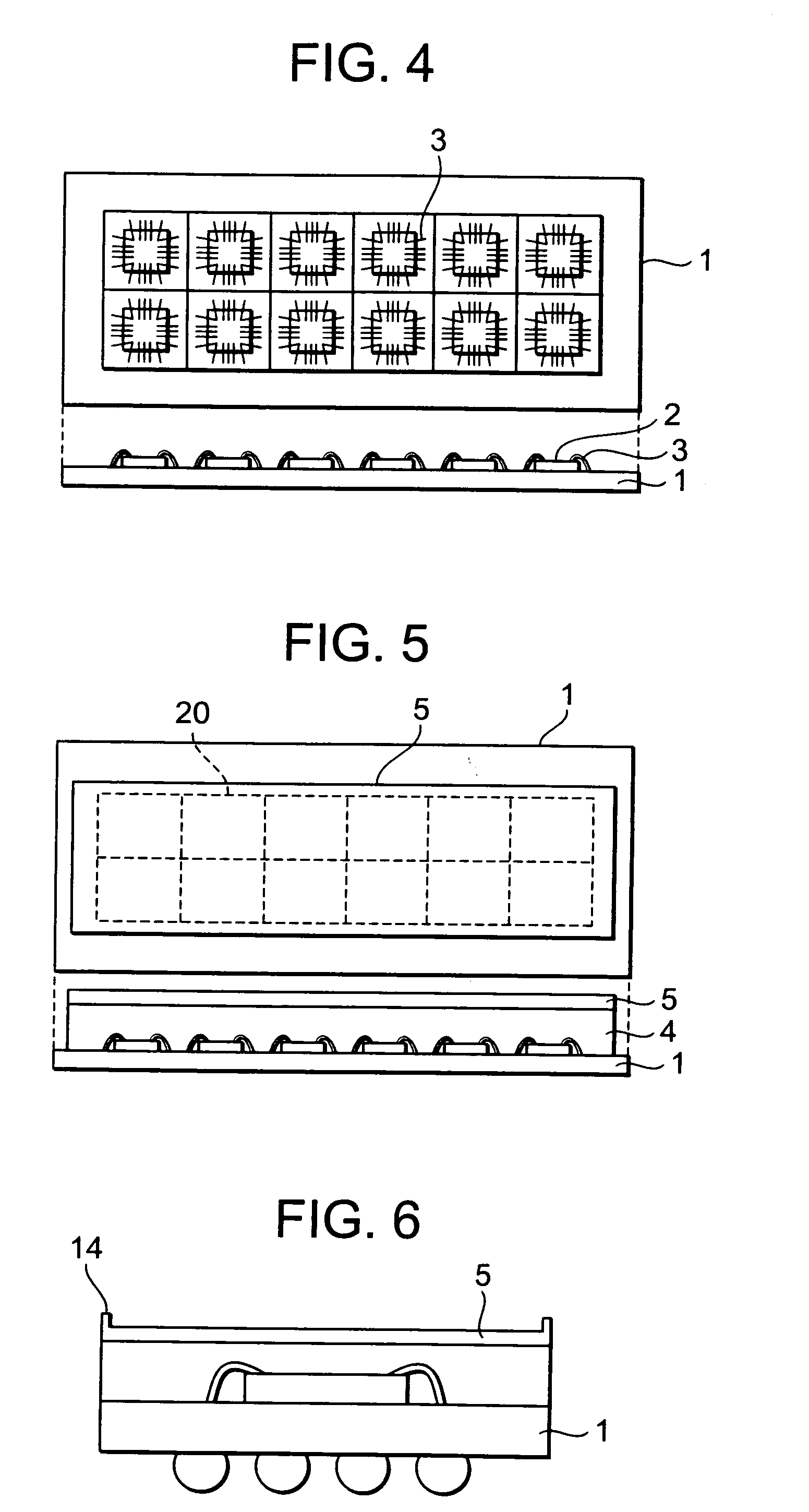
[0058]The semiconductor device in this first embodiment is configured as shown in FIG. 1. Concretely, the semiconductor device includes a wiring board 1; a semiconductor chip 2 mounted on the principal surface of the wiring board 1; sealing resin 4 that seals the semiconductor chip 2; and a heat spreader 5 disposed on the sealing resin 4. At the back side of the wiring board 1 is formed a group of ball-like electrodes 8.

[0059]The wiring board 1 may be, for example, a glass epoxy substrate formed as a multilayer consisting of an insulation layer and a copper wiring layer. The insulation layer is formed by impregnating resin in glass fiber. The wiring board 1 is, for example, 0.3 mm to 0.6 mm in thickness.

[0060]The sealing resin 4 protects the semiconductor chip 2 and functions to stick the heat spreader 5 to the semiconductor chip 2. The sealing resin 4 i...

Example

Second Embodiment

[0099]Next, there will be described the second embodiment of the present invention. FIG. 14 is a flowchart of the manufacturing processes for the semiconductor device in this second embodiment. In this second embodiment, the order of the ball mounting process (S40) is changed from that in the first embodiment. Others are the same as those in the first embodiment, so that detailed descriptions for them will be omitted here.

[0100]FIGS. 15A through 15D are cross sectional views of the semiconductor device in this second embodiment with the manufacturing processes:

[0101]Just like in the first embodiment, the processings from the step S10 to the step S30 are carried out. After ending the processing in step S30, the step (S51) of shaving from the heat spreader 5 side is carried out (FIG. 15A). After this, the ball mounting step (S40) is carried out (FIG. 15B). Then, the step (S52) of shaving from the wiring board 1 side is carried out (FIG. 15C). After ending the step (S5...

Example

Third Embodiment

[0103]Next, there will be described the third embodiment of the present invention. In this third embodiment, the step (S51) of shaving from the heat spreader 5 side is improved from those in the above first and second embodiments. Others are the same as those in the first and second embodiments, so that detailed descriptions for them will be omitted here.

[0104]FIGS. 16A and 16B are cross sectional views of a semiconductor device in this third embodiment with respect to the step (S51) of shaving from the heat spreader 5 side.

[0105]At first, as shown in FIG. 16A, a coat of resist 13 is applied onto the heat spreader 5 of the resin sealing body 10. Then, an opening is formed in the resist 13 along each portion to be cut off.

[0106]After this, as shown in FIG. 16B, the heat spreader 5 is subjected to chemical etching to be carried out with an etching fluid and by using the resist 13 as a mask. As the etching fluid, for example, a compound aqueous liquid of NH4OH and H2O3 ...


PUM


Abstract

A method for manufacturing a semiconductor device includes cutting a resin sealing body into a plurality of pieces. The resin sealing body includes a plurality of semiconductor chips mounted on a wiring board, a heat spreader disposed above the plurality of the semiconductor chips, and sealing resin filled between the wiring board and the heat spreader. The cutting the resin sealing body includes shaving the resin sealing body from a side of the heat spreader and shaving the resin sealing body from a side of the wiring board. The method prevents the heat spreader from generation of burrs.

Description

BACKGROUND OF THE INVENTION[0001]1. Field of the Invention[0002]The present invention relates to a method for manufacturing a semiconductor device having a heat spreader.[0003]2. Description of Related Art[0004]The ball grid array (BGA) is one of the types of semiconductor devices. In case of this BGA type semiconductor device, semiconductor chips are mounted on a wiring board and sealed there with resin. In recent years, those semiconductor devices have been enhanced to meet the requirements of high density packaging and fast operation, thereby they have come to generate heat more and more. This is why there have been developed semiconductor packages having heat spreaders respectively to release the heat therefrom.[0005]For example, JP-A-2003-249512 discloses a semiconductor package, in which a heat spreader is provided above the mounted semiconductor chips. JP-A-2006-294832 also discloses a method for manufacturing a semiconductor package having such a heat spreader. The MAP (Mold...

Claims


Application Information

Patent Timeline
IPC IPC(8): H01L21/78
CPCH01L21/561H01L2924/01033H01L23/4334H01L24/97H01L2224/16H01L2224/48091H01L2224/48227H01L2224/97H01L2924/01011H01L2924/01013H01L2924/01029H01L2924/15311H01L23/3128H01L2924/01023H01L2924/01006H01L2924/01005H01L24/48H01L2224/85H01L2924/00014H01L2224/16145H01L2924/00011H01L2924/181H01L2924/1815H01L2924/00012H01L2224/0401H01L2224/45099H01L2224/45015H01L2924/207
Inventor SATO, YUKOMAEDA, TAKEHIKOKAWASHIRO, FUMIYOSHI
Owner RENESAS ELECTRONICS CORP
Why Eureka
Try Eureka