System and method of forming a patterned conformal structure

Active Publication Date: 2010-05-06
GENERAL ELECTRIC CO
View PDF39 Cites 44 Cited by
  • Summary
  • Abstract
  • Description
  • Claims
  • Application Information

AI Technical Summary

Benefits of technology

[0005]Embodiments of the invention overcome the aforementioned drawbacks by providing a patterned conformal structure for an electrical system, and method of manuf

Problems solved by technology

This has caused an increase in the complexity and operation of the electrical components found in such devices and a decrease in the amount of space available for such components.
Several challenges arise from such an increase in complexity of the electrical components and decrease in the amount of space available.
The reduction in size of the circuit board also leads to increased congestion on the circuit board such that it is difficult to connect component input/output (IO).
The decreased amount of space available also poses a challenge with respect to radio frequency and electromagnetic interference (i.e., RFI and EMI) between comp

Method used


Image

  • System and method of forming a patterned conformal structure
  • System and method of forming a patterned conformal structure
  • System and method of forming a patterned conformal structure

Examples


Embodiment Construction

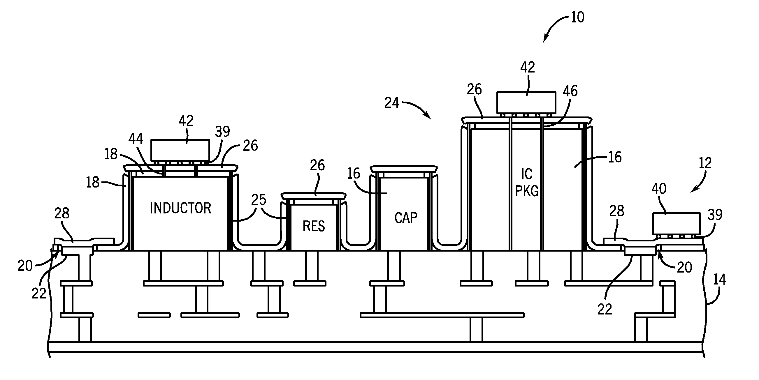
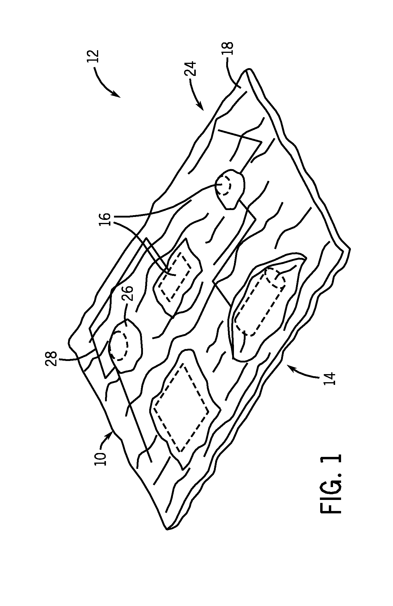
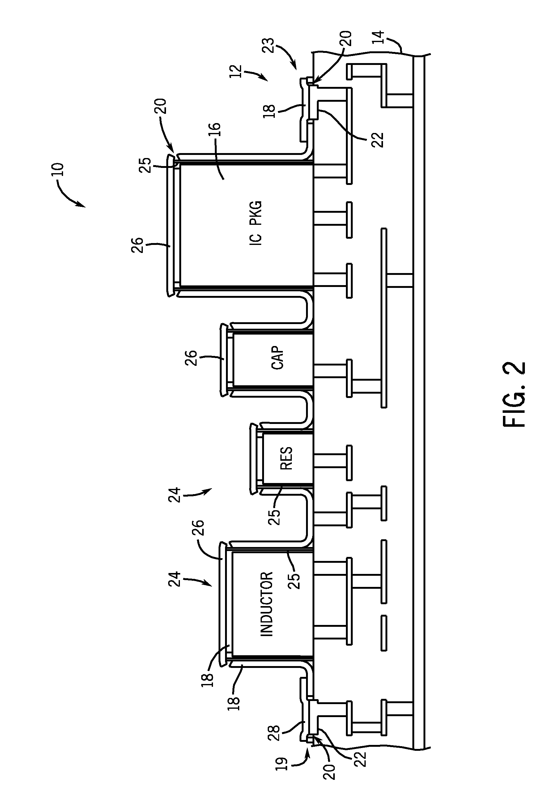
[0015]The present invention provides a patterned conformal shielding and interconnect arrangement or structure. The arrangement is described as being conformal because it is formed to conform or adapt to the shape of the article that it is applied to. While described below with respect to use with a printed circuit board (PCB), it is envisioned that the conformal shielding and interconnect arrangement / structure of the invention may be used in conjunction with other electrical systems and electronic devices.

[0016]Referring to FIG. 1, a perspective view of a patterned conformal structure 10 is shown in accordance with the invention. The patterned conformal structure 10 forms part of a circuit assembly 12, together with a circuit substrate 14, such as a printed circuit board (PCB), flex PCB, rigid flex PCB, or multi-chip module, with circuit components 16 disposed on the circuit substrate 14. The patterned conformal structure 10 is disposed on the circuit substrate 14 and circuit compo...


PUM

PropertyMeasurementUnit
Electrical conductoraaaaaaaaaa
Areaaaaaaaaaaa
Metallic bondaaaaaaaaaa

Abstract

A system and method of forming a patterned conformal structure for an electrical system is disclosed. The conformal structure includes a dielectric coating shaped to conform to a surface of an electrical system, with the dielectric coating having a plurality of openings therein positioned over contact pads on the surface of the electrical system. The conformal structure also includes a patterned conductive coating layered on the dielectric coating and on the contact pads such that an electrical connection is formed between the patterned conductive coating and the contact pads. The patterned conductive coating comprises at least one of an interconnect system, a shielding structure, and a thermal path.

Description

BACKGROUND OF THE INVENTION[0001]Embodiments of the invention relate generally to conformal coatings and, more particularly, to a method and apparatus for forming a patterned conformal structure for an electrical system.[0002]Technological advancements in the area of electronic devices have experienced vast growth in recent years. For example, while cellular phones are becoming smaller and lighter, their features and capabilities are simultaneously expanding. This has caused an increase in the complexity and operation of the electrical components found in such devices and a decrease in the amount of space available for such components. Several challenges arise from such an increase in complexity of the electrical components and decrease in the amount of space available. For example, based on space limitations, circuit boards are reduced in size to an extent that the routing density for the board may be constrained and limited below a desired amount. As every layer of the circuit boa...

Claims


Application Information

Patent Timeline
IPC IPC(8): H05K1/16H05K3/30
CPCH05K1/0218H05K1/181H05K3/284H05K2201/0715H05K2201/09872H05K2201/10515H01L2224/73267H01L2924/19105Y10T29/4913Y10T29/49155Y02P70/611H01L2224/20H01L2224/24195H05K2201/1053H01L2224/16227H01L2224/16235Y02P70/50
Inventor KAPUSTA, CHRISTOPHER JAMESCUNNINGHAM, DONALD PAUL
Owner GENERAL ELECTRIC CO
Why Eureka
Try Eureka