Quantum dot electroluminescent device

a quantum dot and electroluminescent technology, applied in the manufacture of electric discharge tubes/lamps, luminescent coating applications, discharge tubes luminescnet screens, etc., can solve the problems of low efficiency, low efficiency, and low efficiency of phosphors, and achieve the effect of efficient operation

Inactive Publication Date: 2010-05-06
SAMSUNG ELECTRONICS CO LTD
View PDF2 Cites 12 Cited by
  • Summary
  • Abstract
  • Description
  • Claims
  • Application Information

AI Technical Summary

Benefits of technology

[0008]In one embodiment of the present invention, an EL device consists of a simple three active layer construction. A layer of a dielectric material, a traditional EL phosphor layer, and a quantum dot layer are present between an electrode and a transparent electrode. The EL device is operated efficiently by an AC source. In this case quantum dots which emit in the visible spectrum are used. The EL device is fully color-tunable by altering the composition and / or thickness of the layers.
[0011]The semiconductor nanocrystals, or quantum dots more specifically, useful in the present invention are described in the commonly-owned application Ser. Nos. 11 / 125,120 and 11 / 125,129. These quantum dots comprise a core semiconductor with a thin metal layer to protect from oxidation and to aid in lattice matching, and a shell to enhance the luminescent properties, especially for the II-VI or III-V materials. Non-limiting examples of semiconductor nanocrystal cores include ZnS, ZnSe, ZnTe, CdS, CdSe, CdTe, HgS, HgSe, HgTe (II-VI materials), PbS, PbSe, PbTe (IV-VI materials), AIN, AlP, AlAs, AlSb, GaN, GaP, GaAs, GaSb, InN, InP, InAs, InSb, InGaP (III-V materials), CuInGaS2, CuInGaSe2, AgInS2, AgInSe2, and AuGaTe2 (I-III-VI materials). The metal layer is often formed of Zn or Cd, and the shell may be of the same material as the core or any of the above listed core materials.

Problems solved by technology

However, traditional EL phosphors have limited the color range to blue and green in most cases.
However, these tend to be far less efficient and less bright than the traditional EL panels.
Other EL panels have used combinations of orange and blue phosphors to produce white light, typically also with a low efficiency.
These devices are often inorganic / organic hybrids with electrodes of different work functions and suffer severe drawbacks, including grain boundary issues and oxidation of both the DC electrodes and the doped quantum dots.
Doped quantum dots are also more difficult to make and less uniform than those produced by standard quantum dot synthesis.

Method used


Image

  • Quantum dot electroluminescent device
  • Quantum dot electroluminescent device

Examples


example 1

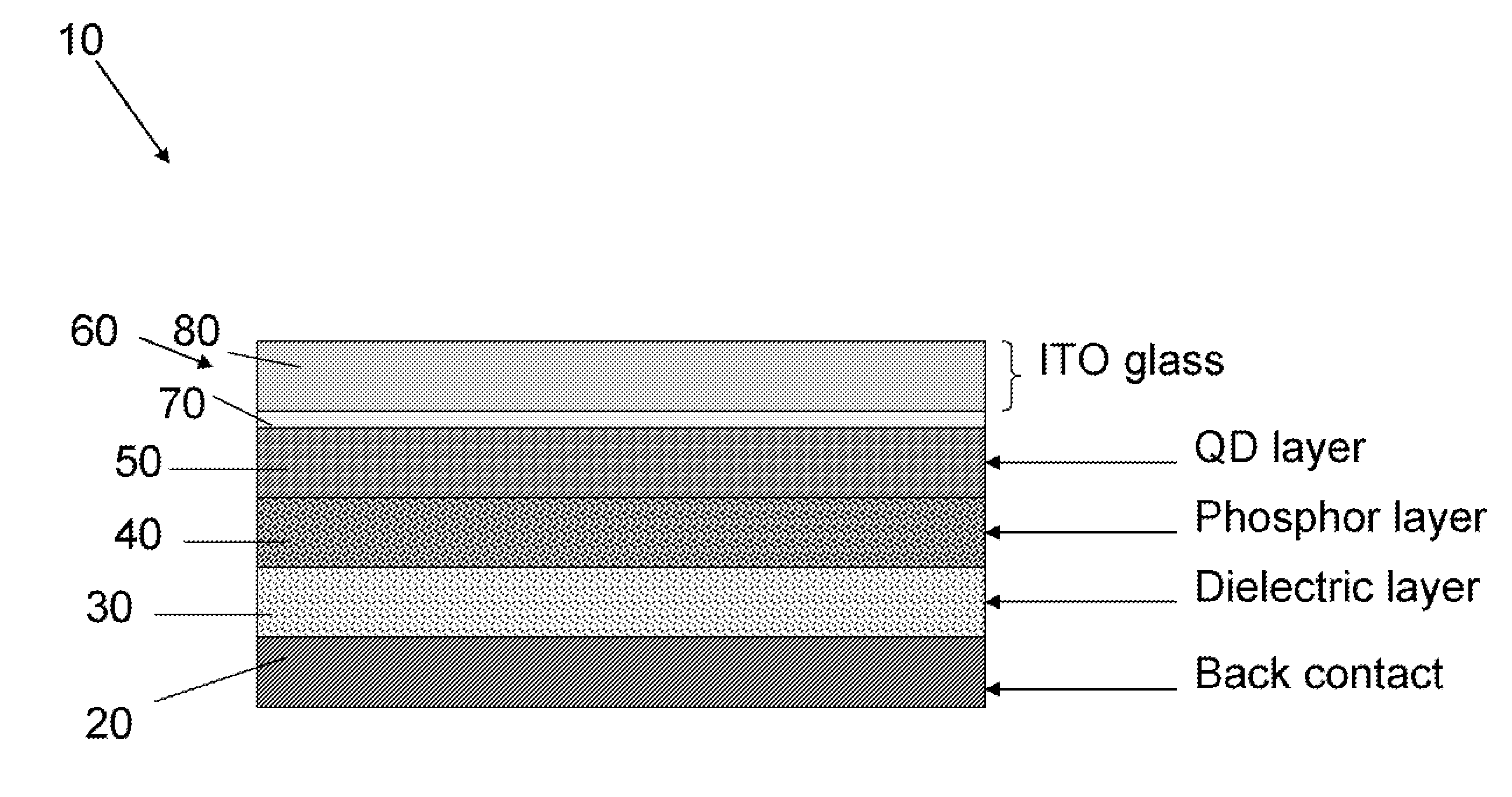
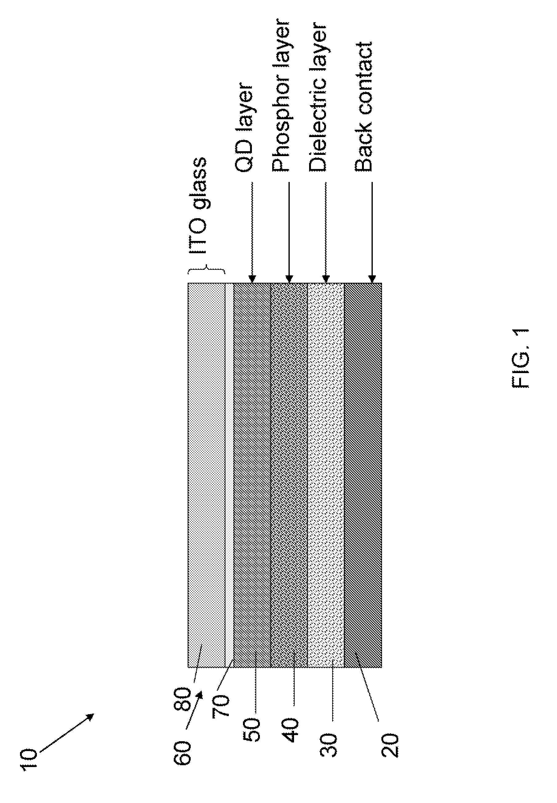
[0023]First, a small piece of ITO glass is obtained, the ITO glass being about the same size as a microscope slide. A quantum dot dispersion in ECPVF is prepared by mixing 100 mg of 625 nm emitting CdSe / ZnS quantum dots (previously synthesized) per 1 mL of ECPVF. The resulting 100 mg / mL dispersion is blade-coated onto the ITO glass. Next, GG65 phosphor from OSRAM-Sylvania is mixed with ECPVF to a concentration of 100 mg / mL and blade-coated onto the quantum dot layer. BaTiO3 is combined with ECPVF to a concentration of 50 mg / mL and blade-coated onto the phosphor layer. A silver conductive paste is then blade coated onto a piece of glass, which is pressed onto the BaTiO3 layer with a wire connected. The wire from the back contact and a wire attached to the ITO glass are connected to a power source and results in a red-emitting EL panel.


PUM


Abstract

An EL device is presented which consists of a simple three active layer construction. A layer of a dielectric material, a traditional EL phosphor layer, and a quantum dot layer are present between an electrode and a transparent electrode. The EL device is operated efficiently by an AC source. Quantum dots which emit in the visible spectrum are used. The EL device is fully color tunable by altering the composition and thickness of the layers.

Description

CROSS-REFERENCE TO RELATED APPLICATIONS[0001]The instant application claims the benefit of co-pending U.S. Provisional Patent Application No. 61 / 107,005, filed 21 Oct. 2008, which is hereby incorporated herein.TECHNICAL FIELD[0002]The present invention relates to a novel electroluminescent (EL) device which incorporates semiconductor nanocrystals, or more specifically quantum dots, into an active layer so as to achieve a better color gamut than traditional EL devices.BACKGROUND OF THE INVENTION[0003]Thick film electroluminescent (EL) displays have been used in many industries. They were commonly used in many military applications including aviation electronics and vehicle panels. They have also found some use in signage applications and decorative lighting. However, traditional EL phosphors have limited the color range to blue and green in most cases. Some thick film EL devices utilize a cascade energy transfer from an underlying blue phosphor with dyes to produce orange to red ligh...

Claims


Application Information

Patent Timeline
Patent Type & Authority Applications(United States)
IPC IPC(8): H01J1/62H01J9/22
CPCC09K11/02C09K11/565C09K11/883H05B33/14H05B33/22
Inventor YANG, SAN MINGSANCHEZ, LUIS A.
Owner SAMSUNG ELECTRONICS CO LTD
Why Eureka
Try Eureka