
Circuit design device for conducting failure analysis facilitating design

a technology of circuit design and failure analysis, which is applied in the direction of cad circuit design, error detection/correction, instruments, etc., can solve the problems of insufficient resolution of failure analysis device, failure analysis has been becoming more and more difficult, and the fault probability of the fault probability of the selected equivalent fault class is reduced

Inactive Publication Date: 2010-05-06
RENESAS ELECTRONICS CORP
View PDF4 Cites 6 Cited by
  • Summary
  • Abstract
  • Description
  • Claims
  • Application Information

AI Technical Summary

Benefits of technology

[0026]As described above, in the circuit design system described in Patent Document 1, elements having observation point functions need to be added to improve failure analyticity. This might lead to an increase in a chip area.
[0036]a placement deciding unit for deciding placement of the elements and the interconnections so as to decrease the fault probability of the selected equivalent fault class.
[0037]With the circuit design device according to the exemplary aspects of the present invention, it is possible to facilitate a failure analysis while avoiding an increase in a chip area, in circuit designing. This is because the circuit design device of the present invention can lower the failure analysis difficulty without inserting an observation point.

Problems solved by technology

Semiconductor integrated circuits manufactured in a manufacturing process of semiconductor integrated circuits include defective products.
However, with miniaturization of the semiconductor integrated circuits in recent years, the failure analysis has been becoming more and more difficult.
This is because the resolution of a failure analysis device is not high enough for the element size of the miniaturized semiconductor integrated circuit.
However, using light in an infrared region, these optical failure-analysis devices cannot obtain a resolution of sub-microns or smaller due to the effect of a diffraction limit.
However, in recent years, as the number of interconnection layers has increased, and the target interconnections to be analyzed are often not exposed, application of the EB analyzer is difficult.
However, when a fault part includes many equivalent faults, the fault diagnosis cannot identify a true fault part and extracts multiple fault candidates.
However, if the number of fault candidates is large, then enormous man-hours are necessary, and thus the failure analysis work takes huge time.
In addition, a fault part in the equivalent fault group cannot be identified by measurement from outside.
This might lead to an increase in a chip area.
Thus, in the circuit design system described in Patent Document 1, a large number of man-hours are needed to insert observation points, which may lead to higher cost of the failure analysis.

Method used


Image

  • Circuit design device for conducting failure analysis facilitating design
  • Circuit design device for conducting failure analysis facilitating design
  • Circuit design device for conducting failure analysis facilitating design

Examples


exemplary embodiment 1

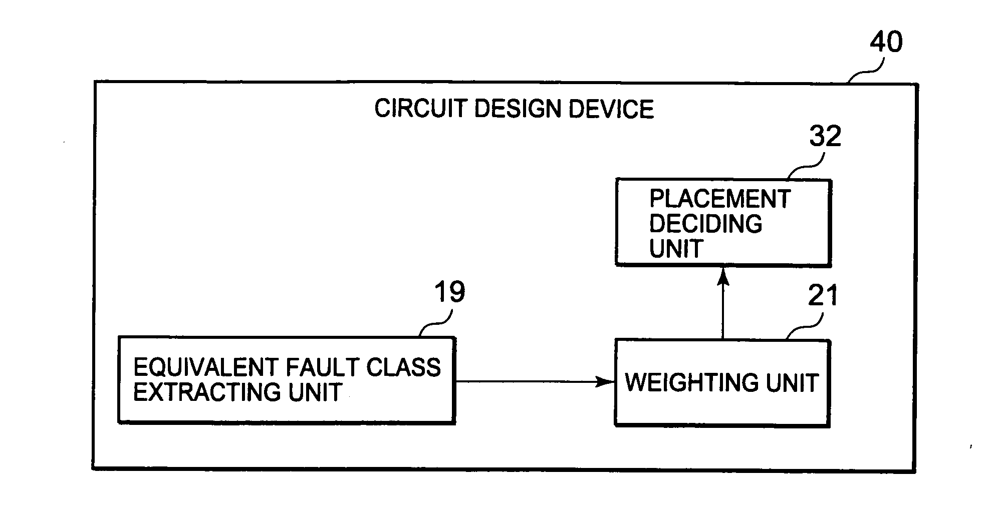
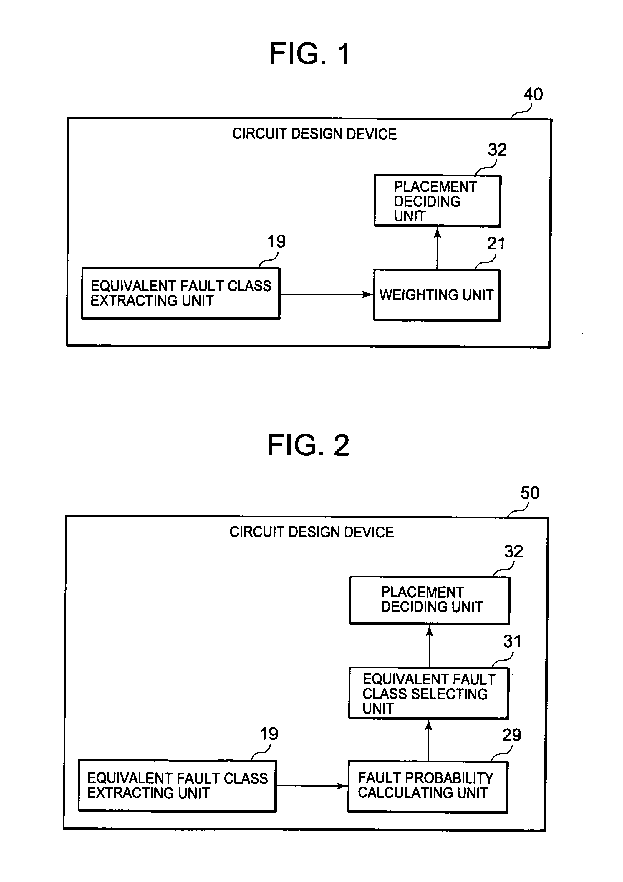
[0047]A circuit design device according to a first exemplary embodiment of the present invention will be described with reference to the drawings. The circuit design device according to the first exemplary embodiment decides the placement of elements and interconnections included in a circuit, on the basis of connection information of the circuit. With reference to FIG. 1, a circuit design device 40 includes an equivalent fault class extracting unit 19, a weighting unit 21, and a placement deciding unit 32.

[0048]The equivalent fault class extracting unit 19 extracts one or more equivalent fault classes each of which is a class having, as members, equivalent fault interconnections that are interconnections mutually causing an equivalent fault in the circuit. The weighting unit 21 gives a greater weight to the equivalent fault class or the equivalent fault interconnections included in the equivalent fault class, as the number of the equivalent fault interconnections that is the number...

exemplary embodiment 2

[0056]A circuit design device according to a second exemplary embodiment of the present invention will be described with reference to FIG. 2. The circuit design device of the second exemplary embodiment decides placement of elements and interconnections included in a circuit, on the basis of connection information of the circuit. With reference to FIG. 2, a circuit design device 50 includes an equivalent fault class extracting unit 19, a fault probability calculating unit 20, an equivalent fault class selecting unit 31, and a placement deciding unit 32.

[0057]The equivalent fault class extracting unit 19 extracts one or more equivalent fault classes each of which is a class having, as members, equivalent fault interconnections that are interconnections mutually causing an equivalent fault in the circuit. The fault probability calculating unit 29 calculates a fault probability which is a probability that the equivalent fault class includes a single stuck-at fault. The equivalent fault...

exemplary embodiment 3

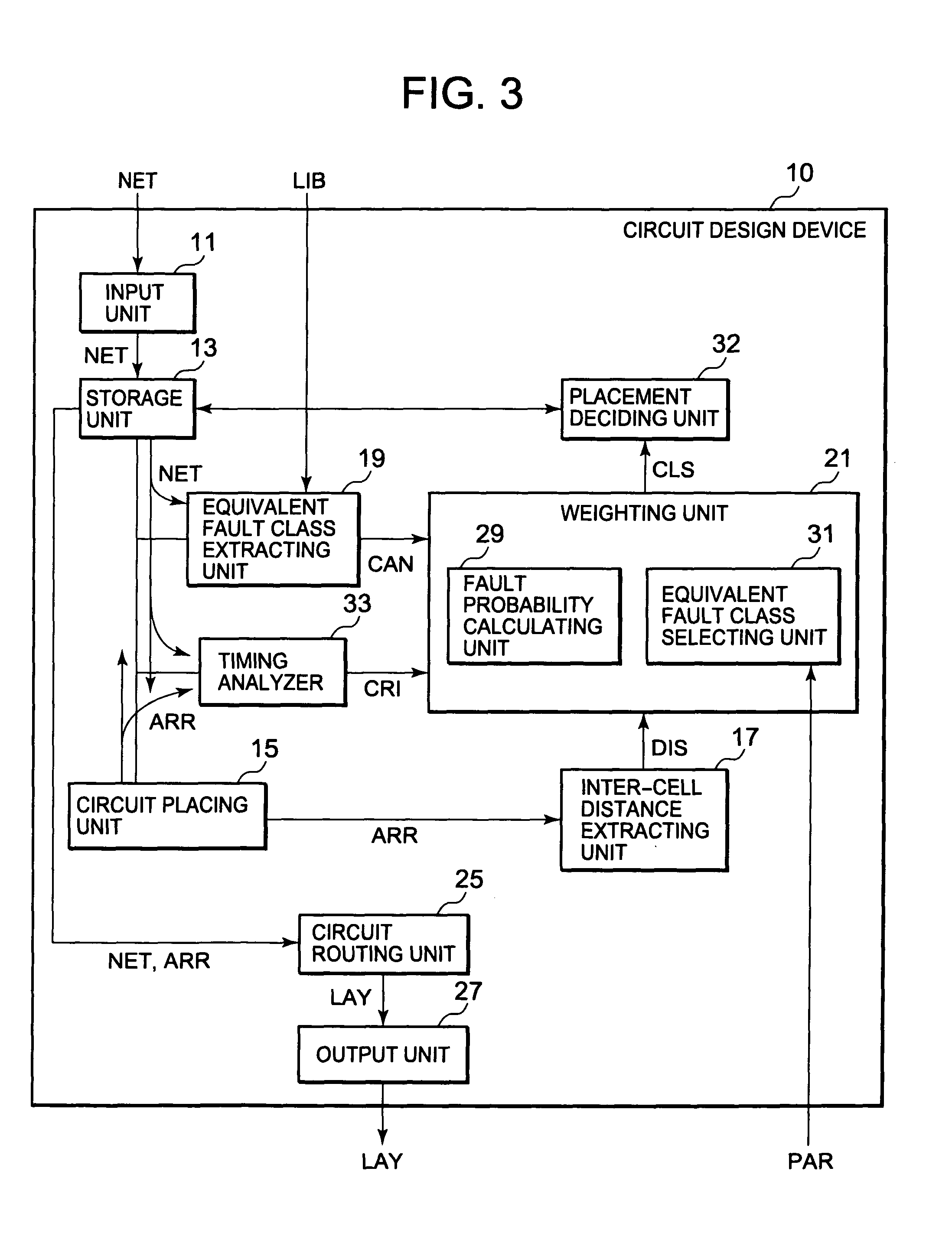
[0074]FIG. 3 is a block diagram showing a configuration of a circuit design device of a third exemplary embodiment. With reference to FIG. 3, a circuit design device 10 includes an equivalent fault class selecting unit 31 and a placement deciding unit 32. In addition, similar to the circuit design system illustrated in FIG. 3 of Patent Document 1, the circuit design device 10 includes a circuit placing unit 15, an equivalent fault class extracting unit 19 (corresponding to the fault candidate extracting unit 109 of Patent Document 1), an inter-cell distance extracting unit 17, a fault probability calculating unit 29 (corresponding to the failure analyticity evaluating unit 119 of Patent Document 1), a circuit routing unit 25, an input unit 11, a storage unit 13, and an output unit 27. Alternatively, the circuit design device 10 may include a timing analyzer 33.

[0075]The operation of the circuit design device 10 according to the third exemplary embodiment will be described. With refe...


PUM


Abstract

A circuit design device decides placement of elements and interconnections included in a circuit, on the basis of connection information of the circuit. The circuit design device includes an equivalent fault class extracting unit, a weighting unit, and a placement deciding unit. The equivalent fault class extracting unit extracts one or more classes (hereinbelow referred to as “equivalent fault classes”) having, as members, interconnections (hereinbelow referred to as “equivalent fault interconnections”) which mutually cause an equivalent fault in the circuit. The weighting unit gives a greater weight to the equivalent fault class or the equivalent fault interconnections included in the equivalent fault class, as the number of the members in the equivalent fault class (hereinbelow referred to as the “number of equivalent fault interconnections”) increases. The placement deciding unit decides placement of the elements and the interconnections so that, among the equivalent classes, an equivalent fault class having a larger number of equivalent fault interconnections would have a lower probability of including a single stuck-at fault.

Description

INCORPORATION BY REFERENCE[0001]This application is based upon and claims the benefit of priority from Japanese Patent Application No. 2008-284660 which was filed on Nov. 5, 2008, the disclosure of which is incorporated herein in its entirety by reference.BACKGROUND OF THE INVENTION[0002]1. Field of the Invention[0003]The present invention relates to a circuit design device, and particularly relates to a circuit design device for an ASIC that is one type of semiconductor integrated circuits, and to a circuit design device for facilitating a failure analysis.[0004]2. Description of Related Art[0005]Semiconductor integrated circuits manufactured in a manufacturing process of semiconductor integrated circuits include defective products. Thus, the defective products are eliminated in a test process and only non-defective products are shipped. Here, a rate of the non-defective products at this time is referred to as a yield. In order to enhance the yield, it is necessary to clarify a cau...

Claims


Application Information

Patent Timeline
IPC IPC(8): G06F17/50
CPCG06F17/5045G06F2217/14G06F30/30G06F30/333
Inventor NONAKA, JUNPEI
Owner RENESAS ELECTRONICS CORP
Learn More