Lightly-doped drains (LDD) of image sensor transistors using selective epitaxy

a technology of image sensor and transistor, applied in the field of image sensors, can solve the problems of low sensitivity, insufficient light collection of photosensitive elements, and limitations of conventional image sensors

Active Publication Date: 2010-05-20
OMNIVISION TECH INC
View PDF14 Cites 20 Cited by
  • Summary
  • Abstract
  • Description
  • Claims
  • Application Information

AI Technical Summary

Problems solved by technology

Conventional image sensors suffer from some limitations.
The smaller photosensitive element area can lead to lower sensitivity.
If the photosensitive element has a relatively low sensitivity, the photosensitive element may not collect enough light.
The result is that the reproduced image can be too dark and noisy.
Low sensitivity and reduced full well capacity can in turn lead to lower dynamic range and lower signal-to-noise ratio.
However, even with sharing, the pixel transistors still take up sizable space of the limited device area.
If the design rules associated with these minimum distances are not adhered to, areas that should be implanted might not be implanted and areas that should not be implanted might accidentally be implanted.
As a result of the design rules, the isolation distance between the photosensitive element and the source / drain of the pixel transistors may not be able to be made as small as desired.

Method used


Image

  • Lightly-doped drains (LDD) of image sensor transistors using selective epitaxy
  • Lightly-doped drains (LDD) of image sensor transistors using selective epitaxy
  • Lightly-doped drains (LDD) of image sensor transistors using selective epitaxy

Examples


Embodiment Construction

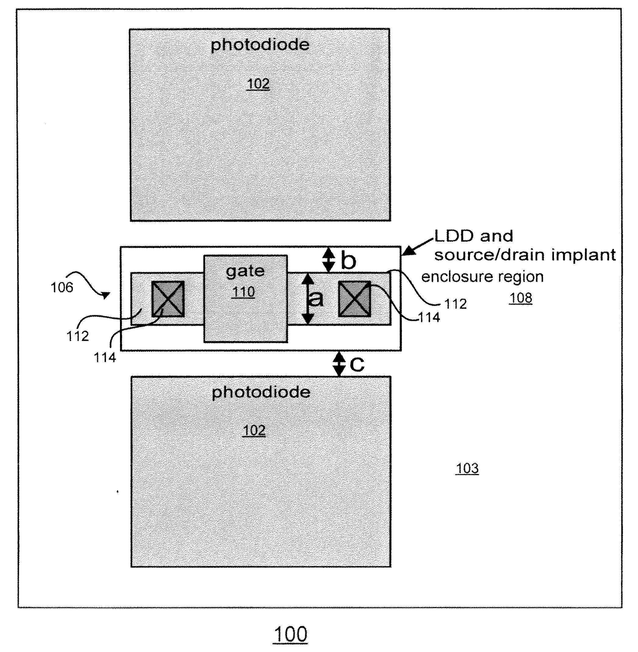
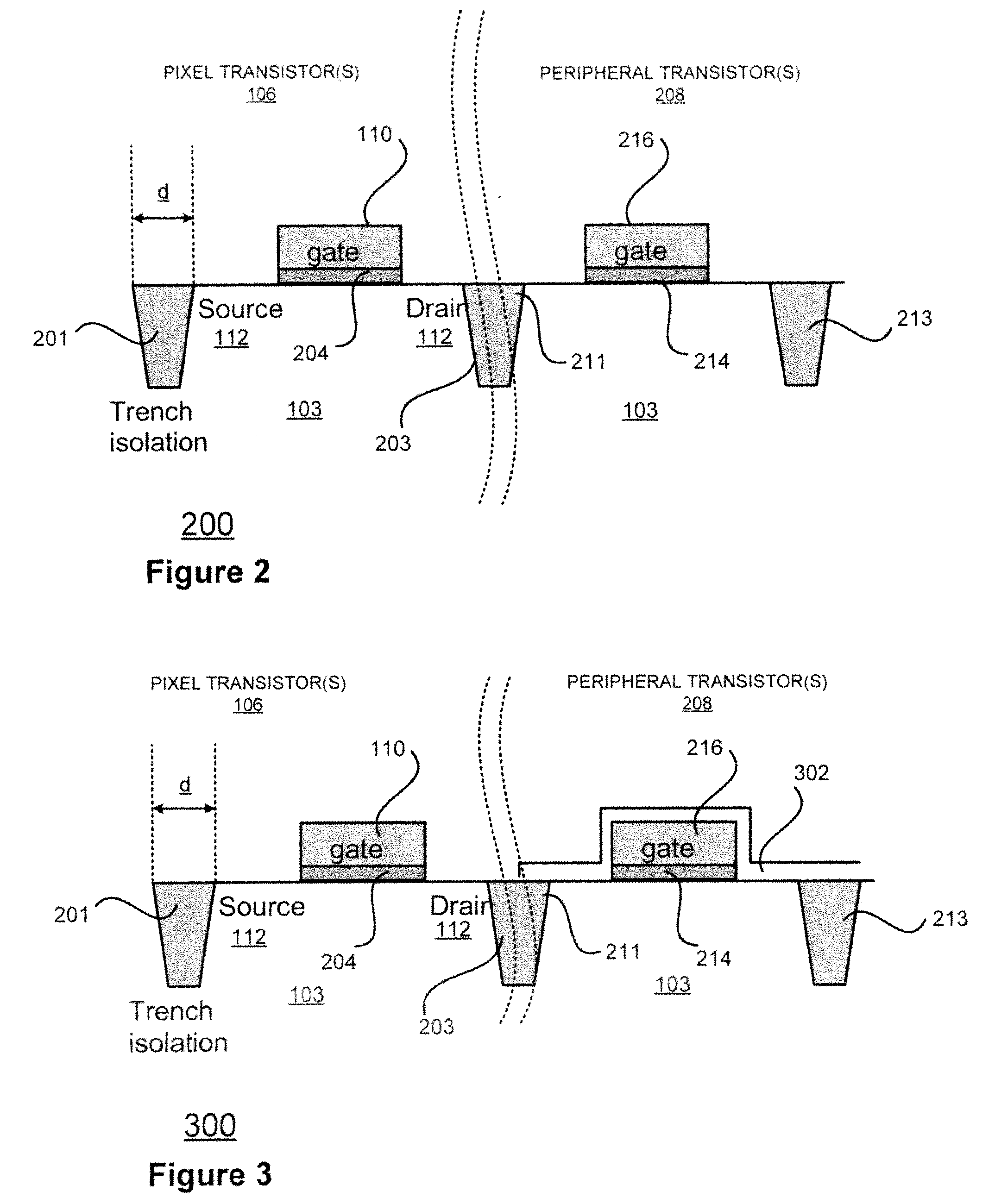
[0018]According to embodiments of the present invention, an image sensor comprises an array of pixels including pixel transistors disposed in or on a semiconductor, e.g., silicon, substrate. In a departure from conventional methods, instead of having LDD regions of the pixel transistors implanted with silicon dopants using a mask, doped silicon may be epitaxially grown in the LDD regions to appropriately dope the LDD regions. Alternatively, a doped sacrificial blanket film may be used to form LDD regions by diffusing the dopants from the film into the LDD regions. If peripheral transistors are disposed on the substrate, a protective oxide is disposed on the peripheral transistors to prevent silicon from being grown on the peripheral transistors during the epitaxial growth process. For some embodiments, the doped silicon may be n-doped silicon. For other embodiments, the doped silicon may be p-doped silicon.

[0019]There are advantages to forming the LDD areas using epitaxial growth ra...


PUM


Abstract

Embodiments of the present invention are directed to an image sensor having pixel transistors and peripheral transistors disposed in a silicon substrate. For some embodiments, a protective coating is disposed on the peripheral transistors and doped silicon is epitaxially grown on the substrate to form lightly-doped drain (LDD) areas for the pixel transistors. The protective oxide may be used to prevent epitaxial growth of silicon on the peripheral transistors during formation of the LDD areas of the pixel transistors.

Description

BACKGROUND[0001]1. Field[0002]Embodiments of the present invention relate to image sensors and in particular, to lightly-doped drain (LDD) implants in image sensor transistors.[0003]2. Discussion of Related Art[0004]A conventional image sensor, which may be fabricated using a complementary metal oxide semiconductor (CMOS) technology or charge coupled device (CCD) technology, includes an array of pixels and associated readout circuitry. The pixel of a typical conventional CMOS image sensor may include a photosensitive element, a micro-lens, one or more light filters, a transfer transistor, a floating diffusion region, reset transistor, source follower, and a row select transistor.[0005]The image sensor generally operates as follows. Light is incident on the micro-lens. The micro-lens focuses the light to the photosensitive element through the light filter. The photosensitive element converts the light into an electrical signal proportional to the intensity of the light detected. The ...

Claims


Application Information

Patent Timeline
Patent Type & Authority Applications(United States)
IPC IPC(8): H01L31/062H01L29/78H01L21/02H01L21/336
CPCH01L27/14609H01L27/14643H01L27/14612H01L29/6659H01L29/66636H01L27/14689
Inventor MAO, DULITAI, HSIN-CHIHRHODES, HOWARD E.VENEZIA, VINCENTQIAN, YIN
Owner OMNIVISION TECH INC
Why Eureka
Try Eureka