Delay adjustment device, semiconductor device and delay adjustment method

a delay adjustment and semiconductor technology, applied in the direction of digital transmission, generating/distributing signals, instruments, etc., can solve the problems of increasing circuit size, increasing circuit size, and difficulty for requestors to determine the timing of data retrieval, so as to reduce chip size and reduce cost

Active Publication Date: 2010-05-20
RENESAS ELECTRONICS CORP
View PDF8 Cites 17 Cited by
  • Summary
  • Abstract
  • Description
  • Claims
  • Application Information

AI Technical Summary

Benefits of technology

[0017]According to exemplary embodiments of the present invention, it is possible to downsize a circuit for adjusting to the flight time. This makes it possible to reduce the chip size, thereby enabling a reduction in cost.

Problems solved by technology

This makes it difficult for the requestor to determine the timing to retrieve data.
The circuit disclosed in Japanese Unexamined Patent Application Publication No. 2005-276396 requires a circuit to preliminarily write a calibration pattern to a memory, and a comparison circuit to compare data read from a memory, resulting in an increase in circuit size.
In these cases, the control circuits use a FIFO, for example, which results in an increase in circuit size.
The present inventor has found a problem that the size of a circuit for adjusting the flight time is increased.

Method used


Image

  • Delay adjustment device, semiconductor device and delay adjustment method
  • Delay adjustment device, semiconductor device and delay adjustment method
  • Delay adjustment device, semiconductor device and delay adjustment method

Examples


first exemplary embodiment

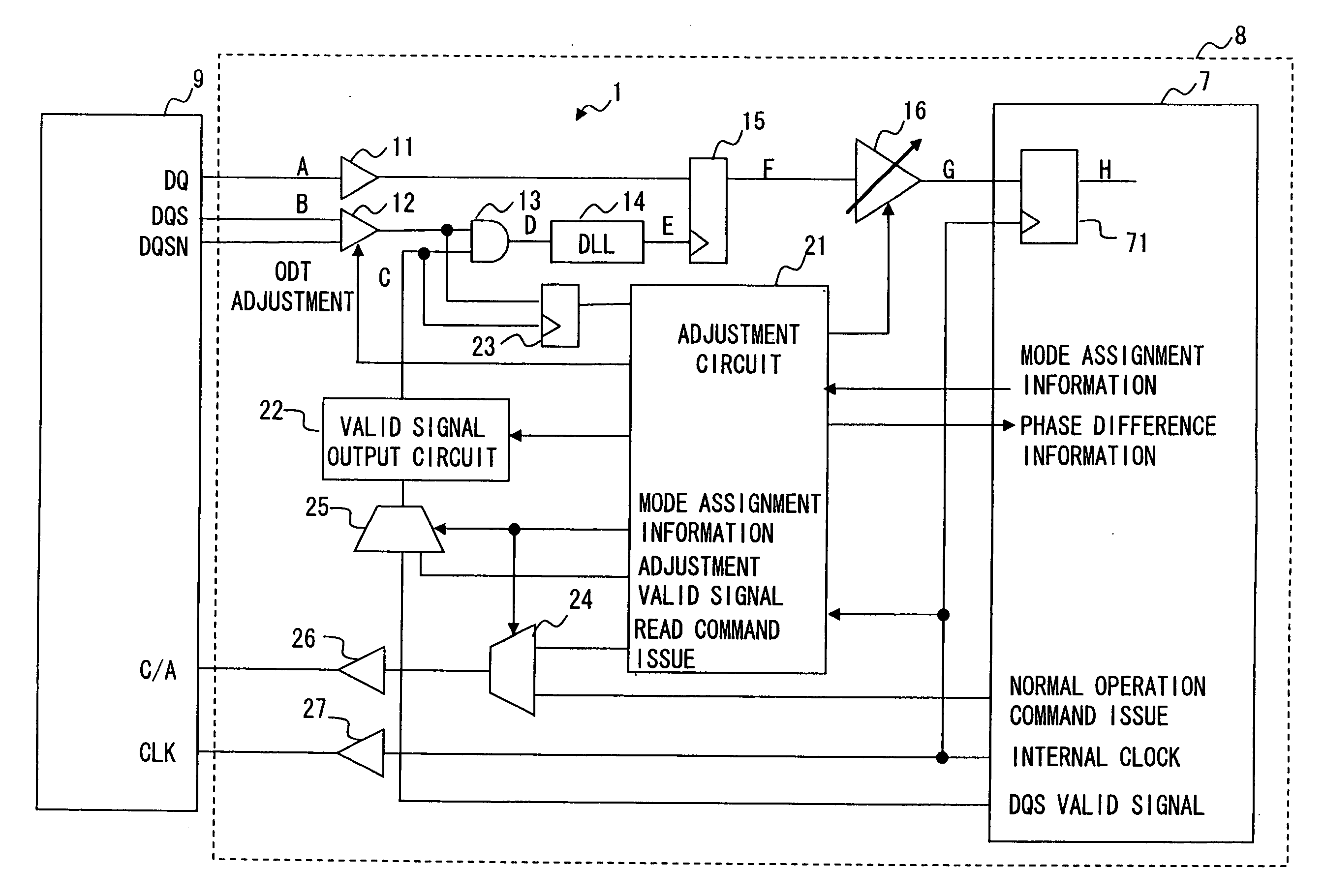
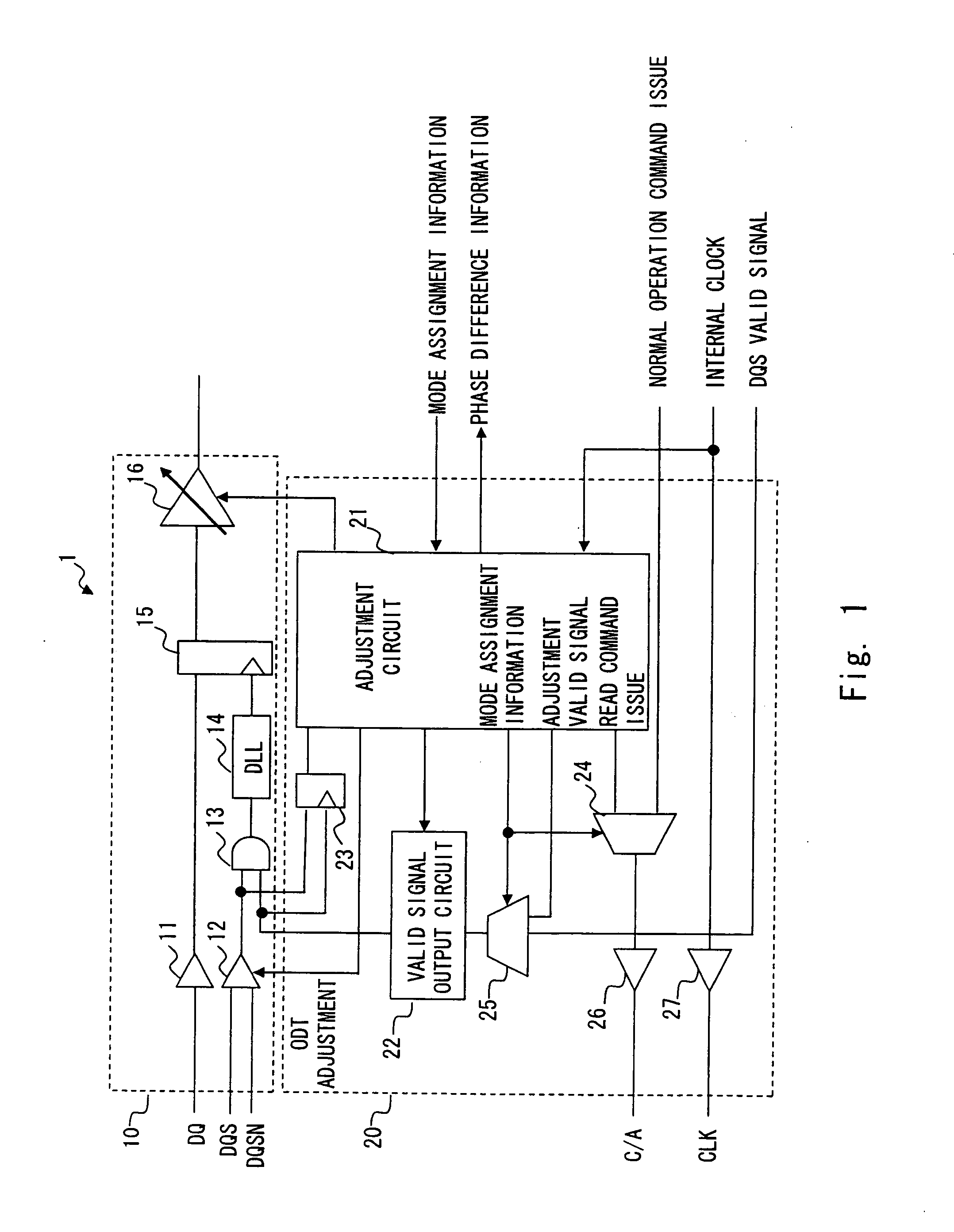
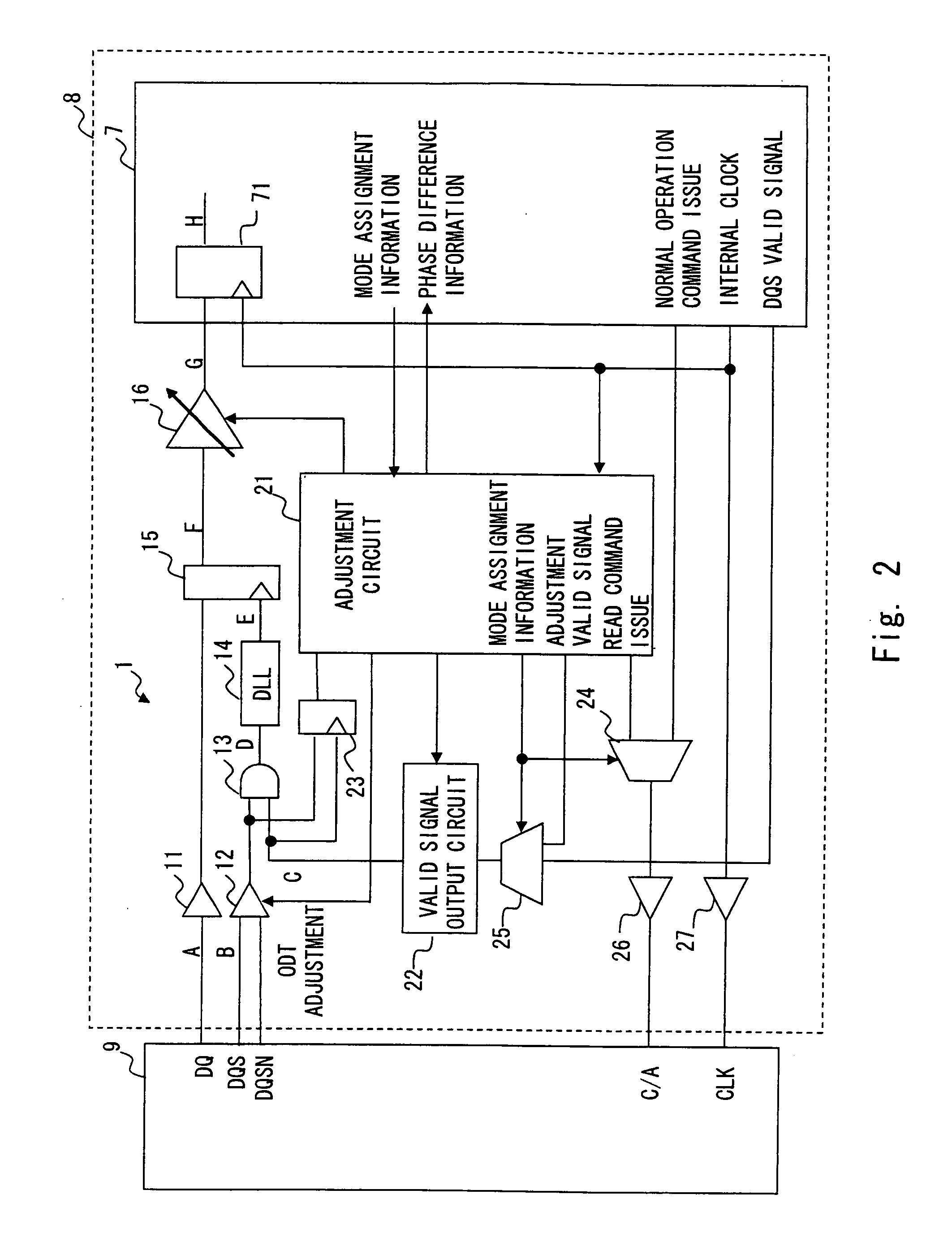
[0030]FIG. 1 is a block diagram showing an example of a configuration of a delay adjustment device (delay adjustment circuit) according to the first exemplary embodiment of the present invention. A delay adjustment circuit 1 includes a data retrieve unit 10 and a control unit 20.

[0031]The data retrieve unit 10 receives the data signal acid data strobe signal from the DDR SDRAM, and outputs the data value of the data signal in accordance with the data strobe signal. The control unit 20 controls the timing for the data retrieve unit 10 to output the data value. Specifically, the data retrieve unit 10 is controlled such that the control unit 20 adjusts a valid period of the data strobe signal.

[0032]The control unit 20 calculates the flight time using the data strobe signal. Specifically, the control unit 20 issues the read command to the DDR SDRAM, and retrieves the value of the data strobe signal (hereinafter also referred to as “strobe value”). The control unit 20 then calculates the...


PUM


Abstract

Provided is a delay adjustment device that contributes to downsizing the circuit that adjusts a flight time. The delay adjustment device is connected to a memory, and adjusts a timing to retrieve data with a data signal and a data strobe signal output from the memory. The delay adjustment device includes a data retrieve unit that receives the data signal and the data strobe signal, and outputs a data value of the data signal in accordance with the data strobe signal; and a control unit that issues a read command to the memory, calculates a flight time, and controls a valid period of the data strobe signal based on the flight time.

Description

BACKGROUND[0001]1. Field of the Invention[0002]The present invention relates to delay adjustment between a memory and a memory controller, and particularly to delay adjustment between a DDR SDRAM (Double Data Rate Synchronous Dynamic Random Access Memory) and a memory controller.[0003]2. Description of Related Art[0004]A DDR SDRAM is a memory including a high-speed transfer function. In particular, the DDR SDRAM can read and write data on both the rising and falling edges of the clock signal for synchronization between circuits. That is to say, the DDR SDRAM inputs and outputs data with twice the frequency of an external clock. Therefore, the DDR SDRAM has a narrower data width (width of determined data), at which data can be reliably read, than that of SDR SDRAM. It is also necessary to notify a timing to read data output from the DDR SDRAM correctly. Thus, the DDR SDRAM uses a data strobe signal (DQS). The data strobe signal is a signal to notify a timing to transfer data. Specifi...

Claims


Application Information

Patent Timeline
Patent Type & Authority Applications(United States)
IPC IPC(8): G11C7/00G11C8/18
CPCG11C7/1066G11C7/22G11C7/222G11C7/225G11C29/02G11C2207/2254G11C11/4076G11C11/407
Inventor ONISHI, SATOSHI
Owner RENESAS ELECTRONICS CORP
Why Eureka
Try Eureka