Semiconductor apparatus manufacturing method and semiconductor apparatus

a manufacturing method and semiconductor technology, applied in the direction of semiconductor devices, semiconductor/solid-state device details, electrical devices, etc., can solve the problems of affecting the quality of semiconductor devices, and end up being very thin or completely etched away, etc., to achieve high yield and highly reliable penetration of electrodes

Inactive Publication Date: 2010-05-27
CANON KK
View PDF12 Cites 17 Cited by
  • Summary
  • Abstract
  • Description
  • Claims
  • Application Information

AI Technical Summary

Benefits of technology

[0015]The prevent invention has been made in view of the above, and an object of the present invention is to provide a semiconductor apparatus with a penetrating electrode and a method of manufacturing the semiconductor apparatus with a penetrating electrode at high yield in which a highly reliable penetrating electrode structure is built by forming an insulating film that has no surface irregularities in bottom etching during a penetrating electrode forming step.

Problems solved by technology

As a result, the insulating film at the corners of the opening portion and the bottom portion is etched at an accelerated rate, and could end up being very thin or completely etched away.
An insulation failure sometimes occurs as a consequence between a penetrating electrode that is formed in the through-hole after the bottom etching and the semiconductor substrate.
Further, the method that uses hard mask eaves has a similar problem in that the protrusion remains after the bottom etching.
The protrusions in the reinforcement insulating film method and the hard mask eaves method create surface irregularities in the insulating film on through-hole inner wall after the bottom etching, and the surface irregularities on the through-hole inner wall present obstacles that leave some spots bare of a barrier layer and a seed layer.
The resultant lowering in yield and reliability of the semiconductor apparatus has been an unsolved problem.

Method used


Image

  • Semiconductor apparatus manufacturing method and semiconductor apparatus
  • Semiconductor apparatus manufacturing method and semiconductor apparatus
  • Semiconductor apparatus manufacturing method and semiconductor apparatus

Examples


embodiment 1

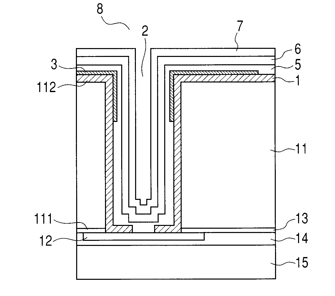
[0051]FIG. 1 is a diagram illustrating a semiconductor apparatus in section according to an embodiment of the present invention. The semiconductor apparatus of the present invention includes the penetrating electrode 8. The electrode pad 12 is formed on the front surface 111 of the semiconductor substrate 11 (or on a surface of the interlayer insulating film 13 in the case where the semiconductor substrate 11 includes the interlayer insulating film 13 formed thereon). The thickness of the semiconductor substrate 11 is 200 μm, for example. The interlayer insulating film 13 is formed by the lamination of SiO2 and SiN in the semiconductor process, for example. Further, components including a semiconductor device (not shown) and wiring (not shown) are connected to the electrode pad 12. The electrode pad 12 has a thickness of, for example, 2.1 μm and the wiring has a thickness of, for example, 0.6 μm. The through-hole 2 with a diameter of, for example, 50 μm is formed in the semiconducto...

embodiment 2

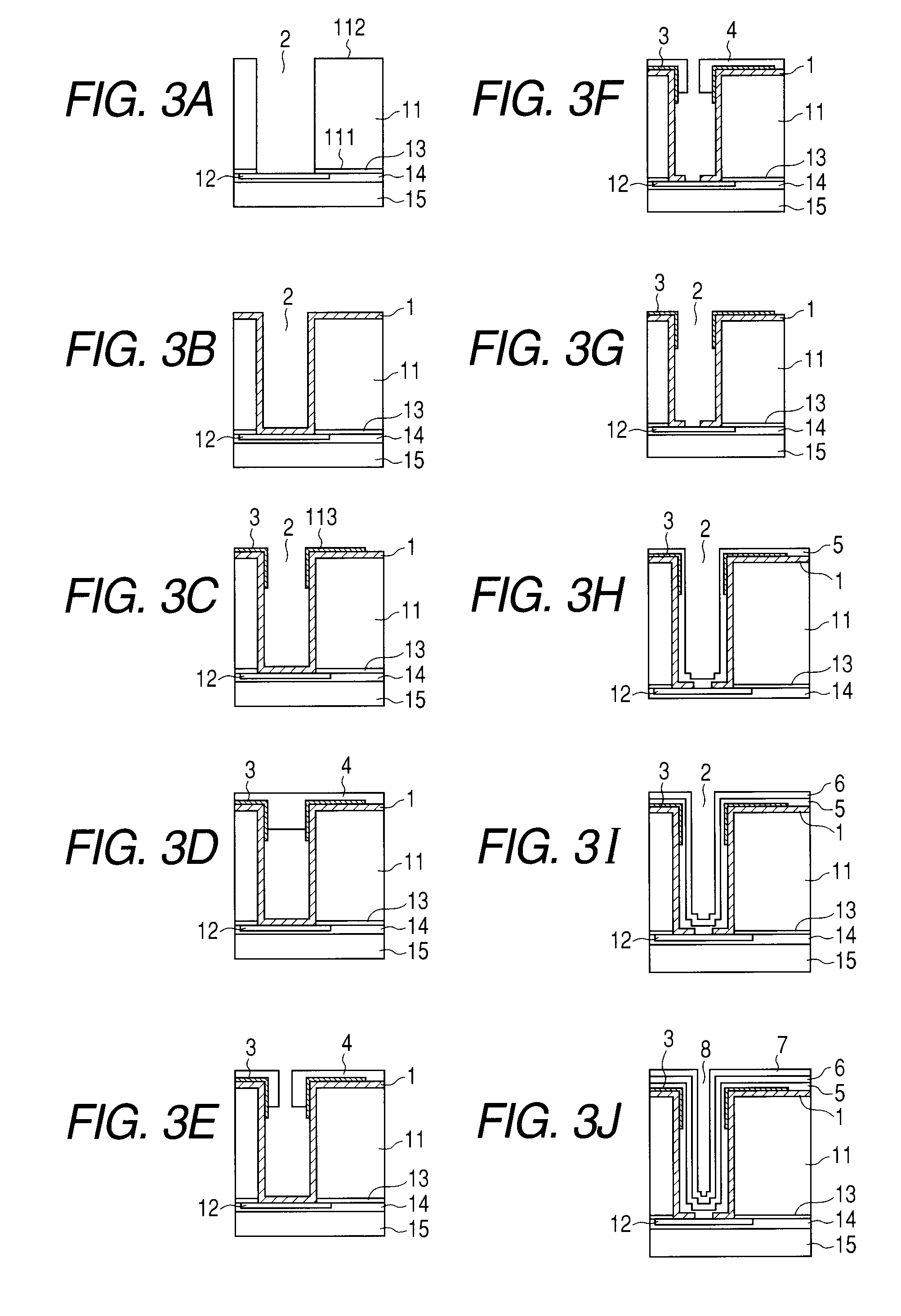
[0053]Embodiment 2 of the present invention is described next. In Embodiment 2, the adhesion securing layer 3 is formed from an inorganic insulating film.

[0054]As illustrated in FIG. 4, sputtering or ECR is used to form an inorganic insulating film as the adhesion securing layer 3 along the opening portion edges of the through-hole 2 and on the entire rear surface of the semiconductor substrate 11. The adhesion securing layer 3 is formed from an inorganic insulator such as SiO2 or SiN. After the adhesion securing layer is formed, the same steps as in Embodiment 1 are executed.

[0055]In a step illustrated in FIG. 5, unnecessary portions of the barrier layer 5 and the seed layer 6 are etched away by tint etching with the use of a dry film.

[0056]The adhesion securing layer 3 which is an inorganic insulating film may be left intact in this step instead of being etched.

[0057]Lastly, a normal dicer is used to cut pieces of the semiconductor apparatus out of a wafer by dicing as in Embodime...


PUM

PropertyMeasurementUnit
thicknessaaaaaaaaaa
thicknessaaaaaaaaaa
thicknessaaaaaaaaaa

Abstract

There is provided a method of manufacturing the semiconductor apparatus, including: forming through-hole which penetrates a semiconductor substrate at a point that corresponds to a location of an electrode pad; forming an insulating film on a rear surface of the semiconductor substrate, including the interior of the through-hole; forming an adhesion securing layer from a metal or an inorganic insulator on a surface of the insulating film at least in an opening portion of the through-hole; forming a resist layer to serve as a mask in bottom etching on the adhesion securing layer; performing bottom etching to expose the electrode pad; removing the resist layer to obtain the insulating film free of surface irregularities that would otherwise have been created by bottom etching; forming a barrier layer, a seed layer, and a conductive layer by a low-temperature process; and performing patterning.

Description

BACKGROUND OF THE INVENTION[0001]1. Field of the Invention[0002]The present invention relates to a semiconductor apparatus manufacturing method and a semiconductor apparatus.[0003]2. Description of the Related Art[0004]The recent reduction in size and improvement in performance of electronic equipment have created a demand for a semiconductor apparatus that is smaller in size and higher in packaging density. Three-dimensional packaging is an effective measure of giving a semiconductor apparatus a smaller size and a higher packaging density. As one of the technologies that constitute the nucleus of three-dimensional packaging, the importance of penetrating electrode technology which is about an electrode connecting a front surface and a rear surface of a semiconductor substrate is increasing.[0005]Raising the packaging density of the semiconductor apparatus with the use of penetrating electrode technology has been practiced. In those practices, wiring is formed on the rear surface of...

Claims


Application Information

Patent Timeline
Patent Type & Authority Applications(United States)
IPC IPC(8): H01L23/48H01L21/768
CPCH01L21/6835H01L21/76898H01L2924/0002H01L2924/00014H01L2224/0401H01L23/481H01L24/02H01L2224/13025H01L2924/01078H01L2924/01079H01L2924/04941H01L2924/12044H01L2924/3025H01L23/49827H01L2224/0557H01L2224/05572H01L2224/05552H01L2924/0001H01L2224/02372H01L2224/02
Inventor MUTA, TADAYOSHI
Owner CANON KK
Why Eureka
Try Eureka