
Multi-Thickness Semiconductor with Fully Depleted Devices and Photonic Integration

a semiconductor and fully depleted technology, applied in the field of semiconductor fabrication, can solve the problems of not allowing for fully depleted soi devices, and not allowing for the ability to modify waveguide thickness independently

Inactive Publication Date: 2010-06-10
BAE SYST INFORMATION & ELECTRONICS SYST INTERGRATION INC
View PDF74 Cites 42 Cited by
  • Summary
  • Abstract
  • Description
  • Claims
  • Application Information

AI Technical Summary

Benefits of technology

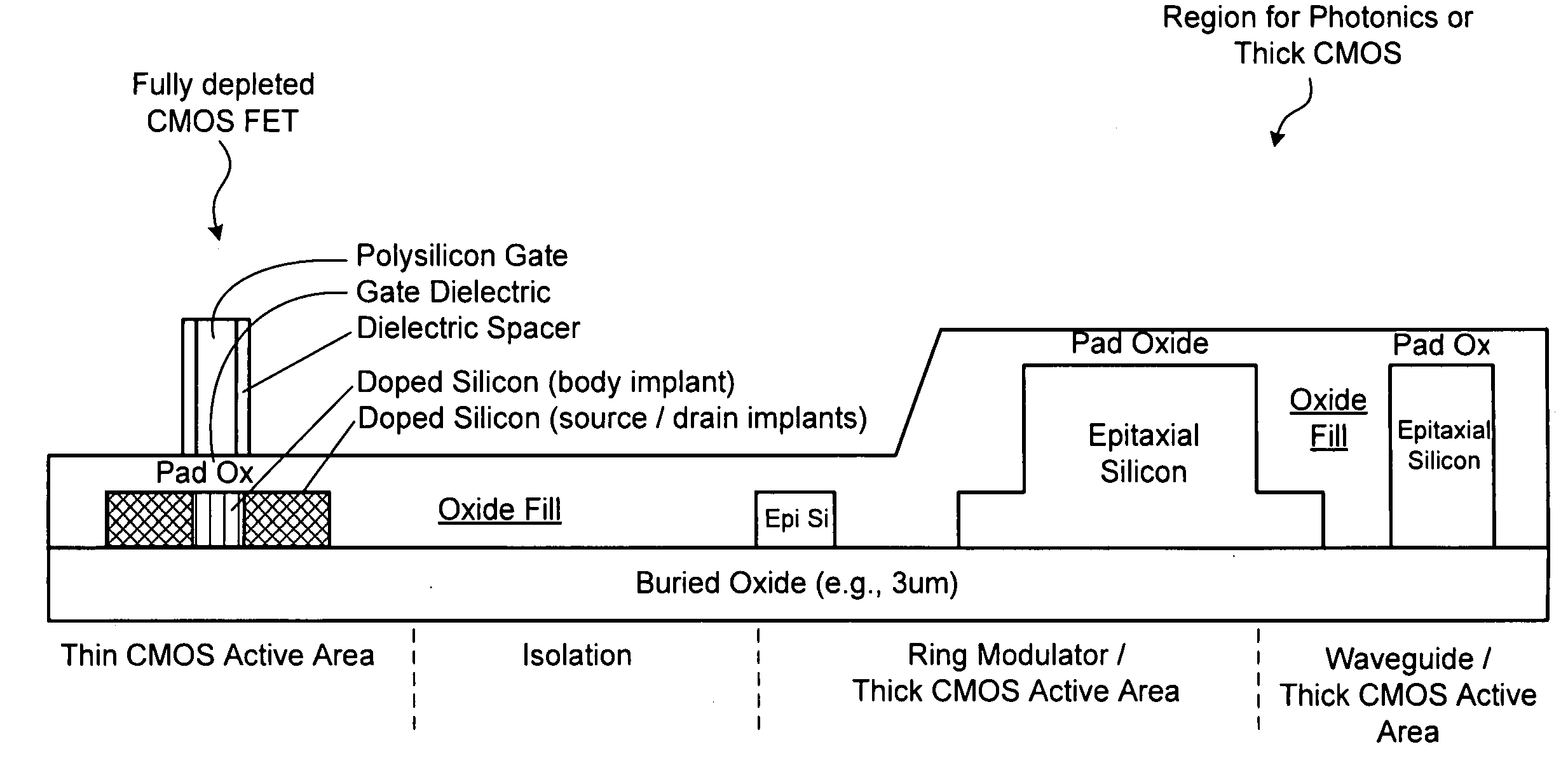
[0008]One embodiment of the present invention provides a semiconductor device. The device includes a semiconductor wafer defining a thin region and a thick region. The device further includes one or more photonic devices and / or partially depleted electronic devices formed on the thick region, and one or more fully depleted electronic devices formed on the thin region. The device may further include an isolation area formed between the thin region and the thick region. The wafer may be, for example, a silicon-on-insulator (SOI) wafer having epitaxial silicon on a thick buried oxide. The partially depleted electronic devices may be, for example, partially depleted CMOS devices, and photonic devices may be, for example, waveguides and / or ring modulators. Note, however, that any number or combination of thin region devices and thick region devices can be used.

Problems solved by technology

Such conventional techniques are associated with a number of disadvantages, including that they do not allow for fully depleted SOI devices.
Nor do they allow for the ability to modify waveguide thickness independently of the CMOS devices.

Method used


Image

  • Multi-Thickness Semiconductor with Fully Depleted Devices and Photonic Integration
  • Multi-Thickness Semiconductor with Fully Depleted Devices and Photonic Integration
  • Multi-Thickness Semiconductor with Fully Depleted Devices and Photonic Integration

Examples


Embodiment Construction

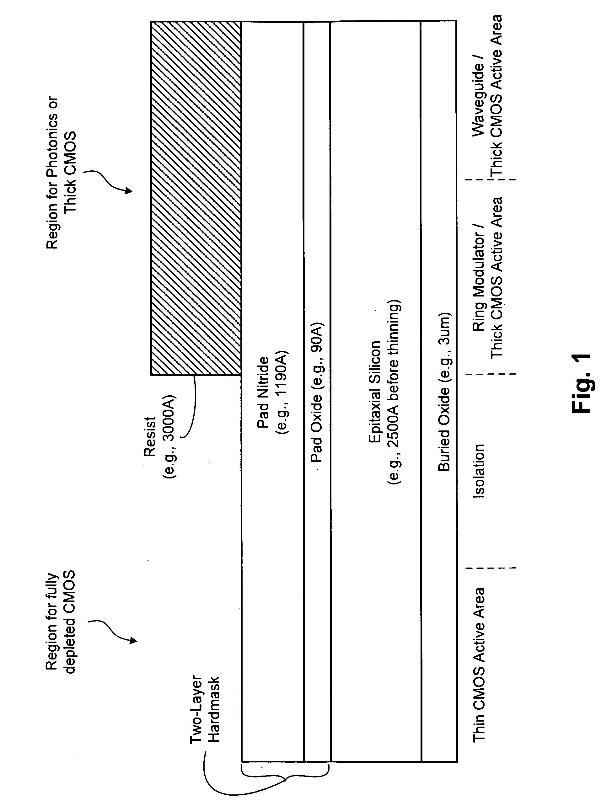
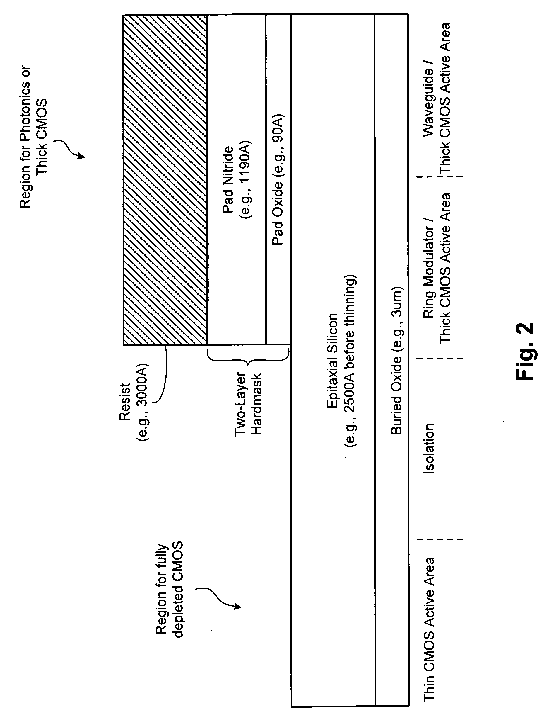
[0012]Techniques are disclosed that facilitate the fabrication of semiconductors including structures and devices of varying thickness. For instance, the techniques can be used to fabricate silicon circuitry that includes fully depleted silicon-on-insulator (SOI) devices (e.g., around 500 A Si thickness), photonic waveguides (e.g., around 2300 A Si thickness), and / or ring modulators (e.g., which may have slab thickness values around 500 to 800 A). Likewise, the techniques can be used to fabricate silicon-based circuitry that includes both channel and ridge waveguide structures. Semiconductor circuitry fabricated with materials other than silicon (e.g., gallium arsenide, indium phosphate, and quartz, sapphire) can equally benefit from the techniques, and numerous circuit configurations will be apparent in light of this disclosure. The techniques are not intended to be limited to particular semiconductor materials or specific types of circuitry / structures; rather, any semiconductor ma...


PUM


Abstract

Techniques are disclosed that facilitate fabrication of semiconductors including structures and devices of varying thickness. One embodiment provides a method for semiconductor device fabrication that includes thinning a region of a semiconductor wafer upon which the device is to be formed thereby defining a thin region and a thick region of the wafer. The method continues with forming on the thick region one or more photonic devices and / or partially depleted electronic devices, and forming on the thin region one or more fully depleted electronic devices. Another embodiment provides a semiconductor device that includes a semiconductor wafer defining a thin region and a thick region. The device further includes one or more photonic devices and / or partially depleted electronic devices formed on the thick region, and one or more fully depleted electronic devices formed on the thin region. An isolation area can be formed between the thin region and the thick region.

Description

RELATED APPLICATIONS[0001]This application is related to U.S. application Ser. No. 12 / 201,807, filed Aug. 29, 2008, and titled “Two-Step Hardmask Fabrication Methodology for Silicon Waveguides” which is herein incorporated by reference in its entirety.FIELD OF THE INVENTION[0002]The invention relates to semiconductors, and more particularly, to a methodology for fabricating semiconductors including structures and devices of varying thickness.BACKGROUND OF THE INVENTION[0003]There are number of waveguide structures that can be used to realize an optical waveguide in silicon, such as ridge and channel waveguides. In such structures, light is typically guided in a high refractive index material (typically referred to as the waveguide core) that is surrounded by a lower index material (typically referred to as the waveguide cladding).[0004]A channel waveguide is usually formed by depositing a high refractive index core material on a low refractive index bottom cladding material. Excess ...

Claims


Application Information

Patent Timeline
Patent Type & Authority Applications(United States)
IPC IPC(8): H01L27/12H01L21/84
CPCG02B6/136H01L21/84H01L27/1203H01L2924/0002H01L2924/00
Inventor HILL, CRAIG M.POMERENE, ANDREW T.CAROTHERS, DANIEL N.CONWAY, TIMOTHY J.VU, VU A.
Owner BAE SYST INFORMATION & ELECTRONICS SYST INTERGRATION INC
Learn More