Substrate processing method and substrate processing apparatus

a substrate processing and substrate technology, applied in the field of substrate processing methods, can solve the problems of take time to complete preliminary heating, etc., and achieve the effects of smooth increase of substrate temperature, and avoiding damage or particle contamination

Inactive Publication Date: 2010-06-10
TOKYO ELECTRON LTD
View PDF3 Cites 9 Cited by
  • Summary
  • Abstract
  • Description
  • Claims
  • Application Information

AI Technical Summary

Benefits of technology

[0022]In accordance with the substrate processing method of the present invention, after performing the first preliminary heating process on the target substrate loaded on the mounting table, the substrate supporting pins of the mounting table are elevated and the second preliminary heating process is then performed while maintaining the target substrate on the substrate supporting pins. In the second preliminary heating process, since the target substrate is supported on the substrate supporting pins not on the mounting table, the temperature of the substrate passes a temperature range in which the substrate is likely to warp in the temperature increasing through the second preliminary heating process. Accordingly, even if the substrate is warped, it is possible to avoid damage or particle contamination thereof.
[0023]Furthermore, the warpage of the substrate can be eliminated during the second preliminary heating process in which the temperature of the substrate is smoothly increased while being supported on the substrate supporting pins. Accordingly, even in case of a large substrate, the warpage of the substrate can securely prevented.
[0024]In addition, by performing the first preliminary heating process while the substrate is mounted on the mounting table, the temperature increasing time in this temperature range becomes shortened, thereby improving a throughput of the processing.

Problems solved by technology

Once the wafer is warped, misalignment of the wafer would be caused while the wafer is being transferred, and a wafer edge portion or the like would come into a contact with the susceptor, resulting in a damage or a particle contamination.
However, since the preliminary heating process is performed in the state the wafer is distanced apart from the mounting table by being sustained on the wafer supporting pins for the purpose of avoiding a rapid temperature rise of the wafer, it takes time to complete the preliminary heating.

Method used


Image

  • Substrate processing method and substrate processing apparatus
  • Substrate processing method and substrate processing apparatus
  • Substrate processing method and substrate processing apparatus

Examples


Embodiment Construction

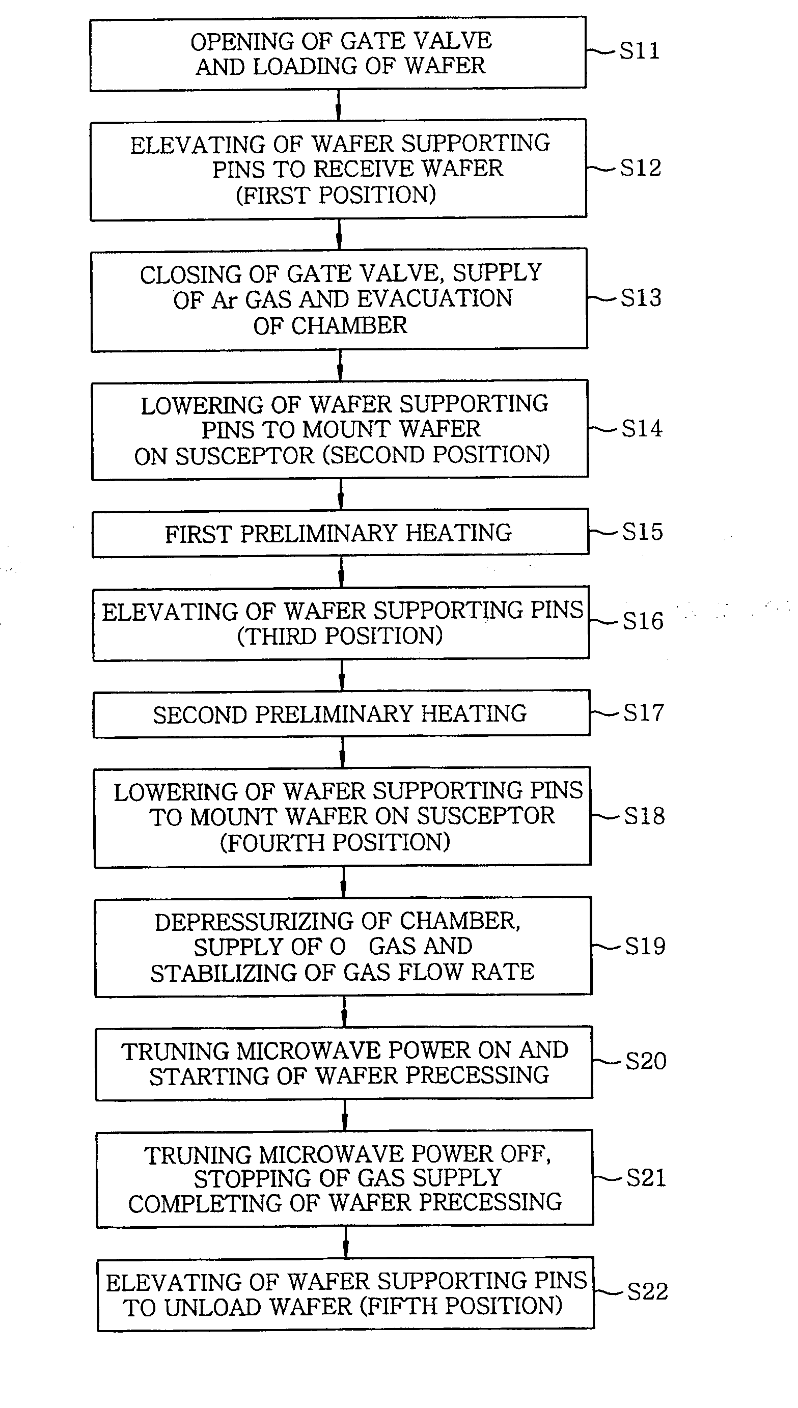
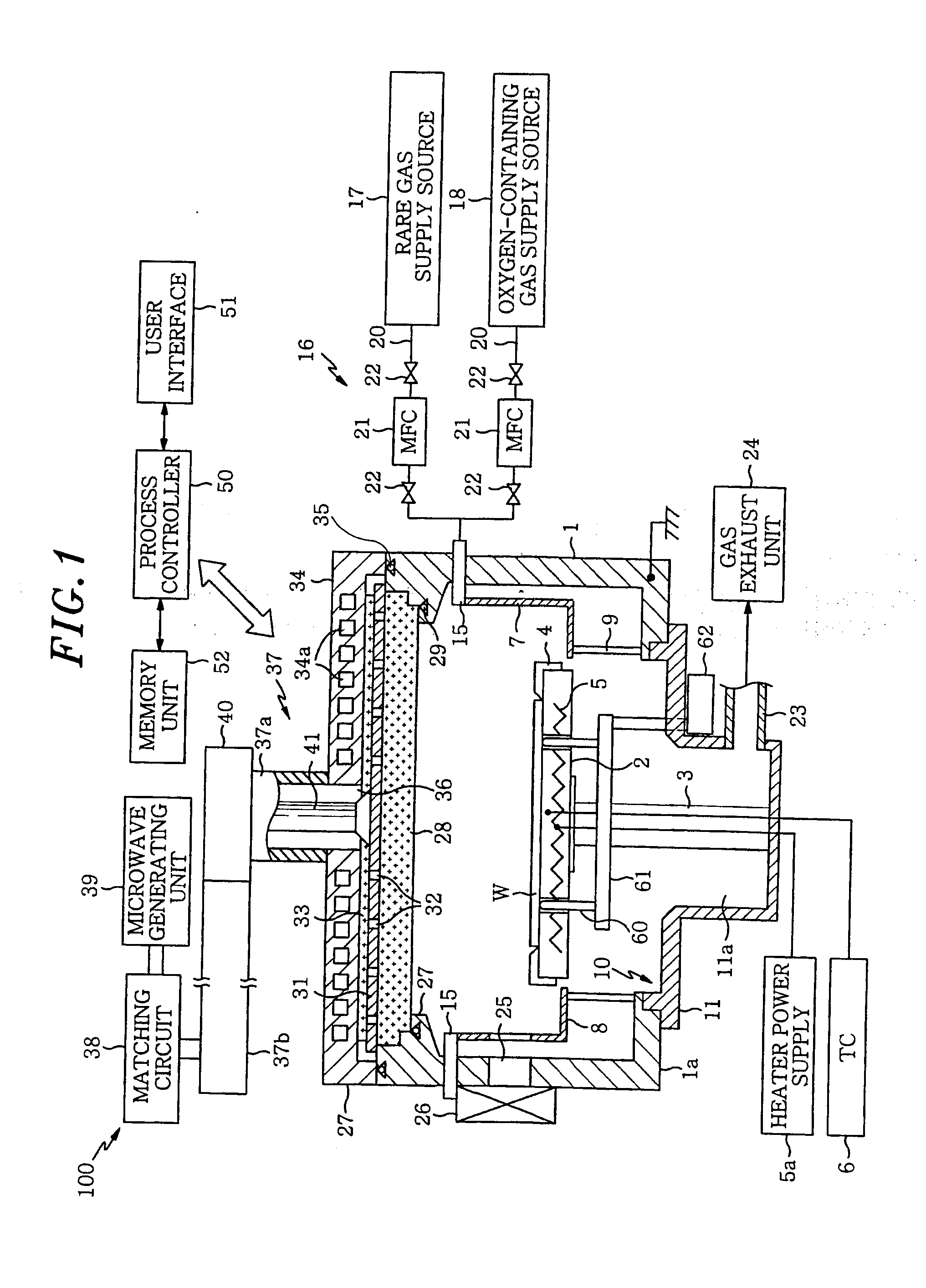
[0037]Hereinafter, an embodiment of the present invention will be described in detail with reference to the accompanying drawings. FIG. 1 provides a schematic cross sectional view showing an exemplary plasma processing apparatus 100 to which the present invention is appropriately applicable. The plasma processing apparatus 100 is configured as a RLSA (Radial Line Slot Antenna) microwave plasma processing apparatus capable of generating a high-density microwave-excited plasma having a low electron temperature by way of generating the plasma while introducing a microwave into a processing chamber through a planar antenna having a number of slots, especially, an RLSA antenna. With this plasma processing apparatus 100, a plasma process can be carried out by using a plasma having a plasma density ranging from about 1×10¹⁰ to 5×10¹² / cm2 and an electron temperature ranging from about 0.7 to 2 eV.

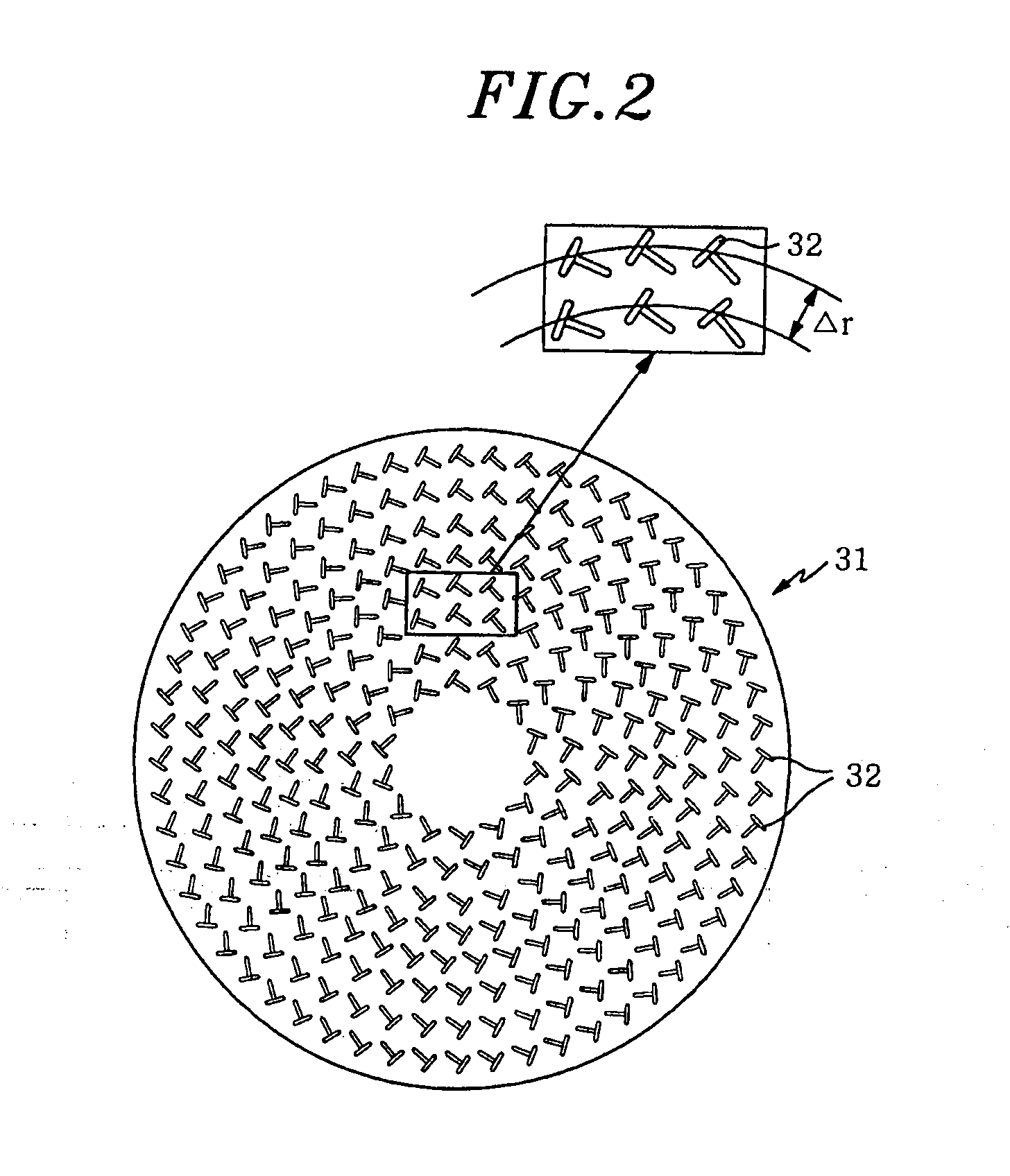
[0038]In the present embodiment, the plasma processing apparatus 100 is configured as a plasma ...


PUM

PropertyMeasurementUnit
temperatureaaaaaaaaaa

Abstract

In a substrate processing method, a substrate to be processed is mounted on a mounting table in a processing chamber of a substrate processing apparatus, and while heating the substrate by a heating unit through the mounting table to a processing temperature of 700° C. or higher, the substrate is processed. The substrate to be processed is loaded into the processing chamber, a first preliminary heating is performed until the substrate reaches a prescribed temperature while being mounted on the mounting table. Then, substrate supporting pins of the mounting table are elevated, and a second preliminary heating is performed in a state where the substrate is held on the substrate supporting pins. Then, the substrate supporting pins are moved down to mount the substrate on the mounting table and a process such as plasma oxidation is performed thereon.

Description

FIELD OF THE INVENTION[0001]The present invention relates to a substrate processing method; and, more particularly, to a substrate processing method for performing, e.g., a film forming process on a target substrate such as a semiconductor wafer.BACKGROUND OF THE INVENTION[0002]A film forming apparatus for performing a film forming process on a semiconductor wafer, which is a target substrate to be processed, by, for example, a chemical vapor deposition (CVD) method includes a susceptor serving as a substrate mounting table for mounting the wafer thereon, and the susceptor has a heating unit therein. Various film forming reactions are carried out while heating the wafer indirectly by means of heating the susceptor. The susceptor is made of a ceramic-based material such as AlN having a high thermal conductivity, and is capable of heating the target substrate up to a processing temperature of, for example, about 700° C. or higher.[0003]Recently, a wafer size has increased to about 200...

Claims


Application Information

Patent Timeline
Patent Type & Authority Applications(United States)
IPC IPC(8): H01L21/302B05C11/00
CPCC23C16/45565C23C16/46H01J37/32192H01L21/67109H01L21/02238H01L21/02252H01L21/31662H01J2237/2001H01L21/20H01L21/205
Inventor TAKATSUKI, KOICHI
Owner TOKYO ELECTRON LTD
Why Eureka
Try Eureka