
Integrated power amplifiers for use in wireless communication devices

a power amplifier and wireless communication technology, applied in the direction of amplifiers with semiconductor devices only, differential amplifiers, amplifiers with semiconductor devices/discharge tubes, etc., can solve the problems of reducing the efficiency of the carrier amplifier, preventing the carrier amplifier from reaching the maximum voltage swing, and not being able to operate the amplifier(s) in linear manner, so as to reduce the amount of chip layout area, reduce the layout area, and shrink the design

Inactive Publication Date: 2010-06-17
SAMSUNG ELECTRO MECHANICS CO LTD +1
View PDF5 Cites 41 Cited by
  • Summary
  • Abstract
  • Description
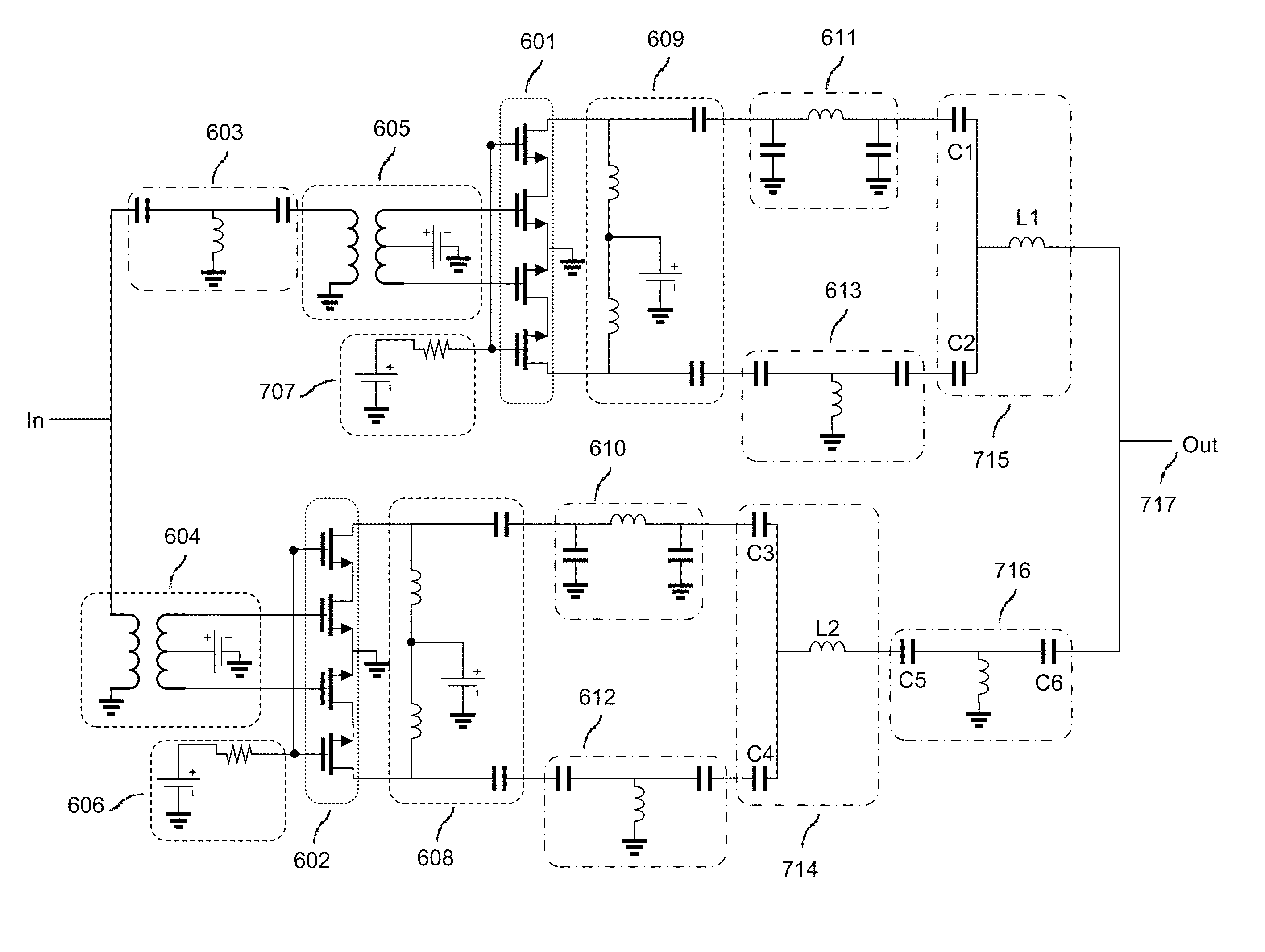
  • Claims
  • Application Information

AI Technical Summary

Benefits of technology

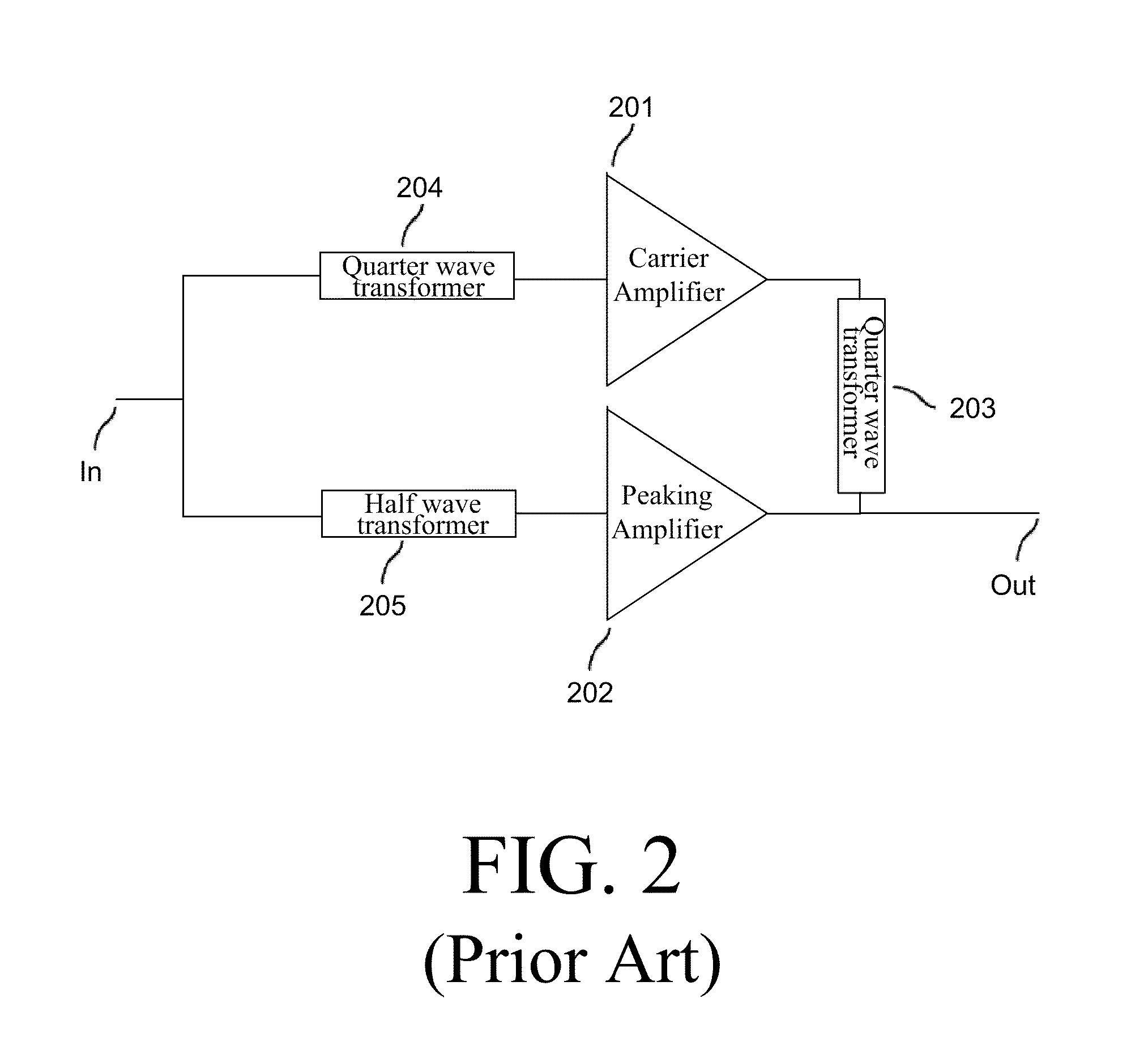
[0009]Example embodiments of the invention may include quarter wave transformers at the inputs of a carrier amplifier to achieve uneven power operation, but the peaking amplifier path transformer elements may be provided at the output side. This example configuration leverages the lower characteristic impedance necessary to the output side in order to reduce the amount of chip layout area consumed. Moreover, according to example embodiments of the invention, the output side balun and one quarter wave transformer may be combined into one structure that includes two quarter wave transformers mutually at or about (“substantially”) 180 degrees out of phase, further shrinking the design and reducing the layout area needed. This is possible with lumped element quarter wave transformers which can achieve negative and positive (at or about) (“substantially”) 90 degree phase shifts dependant on component placement. The configuration used in example embodiments of the invention may result in a compact linear amplifier in a CMOS process with improved efficiency in the back-off region and low quiescent current consumption.

Problems solved by technology

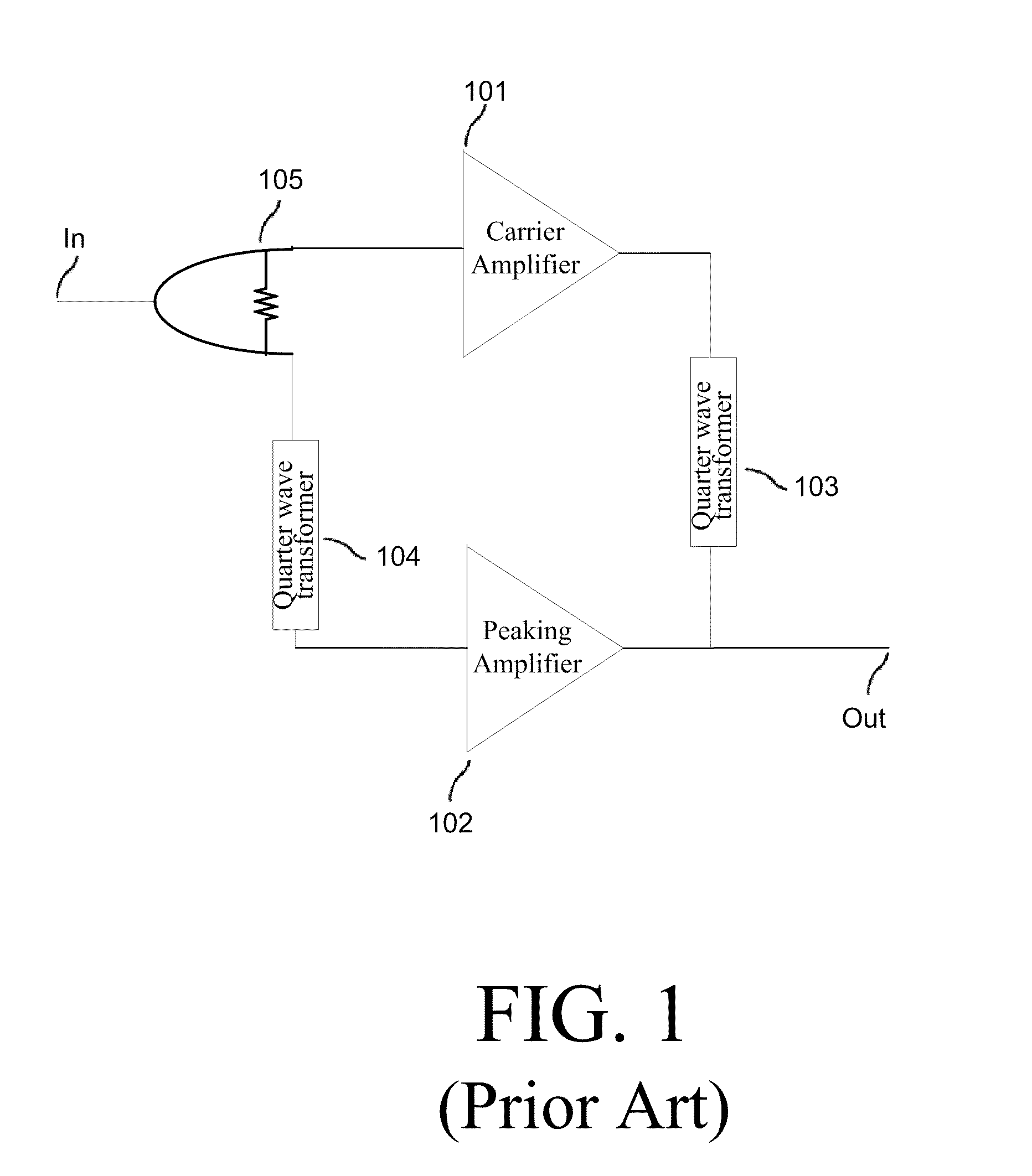
Power amplifiers in mobile handsets are typically stand-alone structures due to the difficulty in simultaneously achieving high power, high efficiency, and high linearity in the low-cost CMOS processes (or structures) used for the rest of the communications circuitry.
In a typically non-linear process (or structure) such as CMOS, such non-linear operation of the amplifier(s) is unacceptable due to stringent linearity and power requirements in modern wireless communication standards.
Moreover, a higher bias point reduces the efficiency of the Doherty amplifier by modulating the load at too low of an input power and thus preventing the carrier amplifier from reaching a maximal voltage swing.
Although uneven power drive appears attractive in terms of efficiency, layout area is not significantly reduced at cellular frequencies since transmission lines are not feasible, and therefore lumped element equivalents must be used.
Furthermore, in CMOS processes (or structures), linearity complications arise making it unattractive to implement dynamically uneven power drive as the desired efficiency gains must be sacrificed.
Another complication in CMOS is low breakdown voltage compared to dominant power amplifier technologies.
This deficiency leads to several topological choices, particularly a differential cascode structure.
In addition to the two lumped element quarter wave transformers necessary for Doherty amplifier operation, the area of these structures makes the topology highly inefficient with respect to layout area.

Method used


Image

  • Integrated power amplifiers for use in wireless communication devices
  • Integrated power amplifiers for use in wireless communication devices
  • Integrated power amplifiers for use in wireless communication devices

Examples


Embodiment Construction

[0024]Embodiments of the invention now will be described more fully hereinafter with reference to the accompanying drawings, in which some, but not all embodiments of the invention are shown. Indeed, these inventions may be embodied in many different forms and should not be construed as limited to the embodiments set forth herein; rather, these embodiments are provided so that this disclosure will satisfy applicable legal requirements. Like numbers refer to like elements throughout.

[0025]Example embodiments of the invention may be directed to an integrated power amplification circuit for a mobile device (e.g., a mobile phone, radio, pager, laptop computer, handheld computer, personal digital assistant device, and the like) with improved efficiency and linearity properties while having minimal impact on circuit size and / or a reduction in integrated layout area consumed. In an example embodiment of the invention, an integrated power amplifier designed for cellular band frequencies in ...


PUM


Abstract

An integrated power amplifier can include a carrier amplifier, where the carrier amplifier is connected to a first quarter wave transformer at the input of the carrier amplifier. In addition, the power amplifier can further include at least one peaking amplifier connected in parallel with the carrier amplifier; a first differential combining structure, where the first combining structure includes a first plurality of quarter wave transformers that are configured to combine respective first differential outputs of the carrier amplifier in phase to generate a first single-ended output signal, and a second differential combining structure, where the second combining structures includes a second plurality of quarter wave transformers that are configured to combine respective second differential outputs of the at least one peaking amplifier in phase to generate a second single-ended output signal, where the first single-ended output signal and the second single-ended output signal are combinable in-phase to provide an overall output.

Description

RELATED APPLICATION[0001]The present application claims priority to U.S. Provisional Application No. 61 / 122,275, filed on Dec. 12, 2008, and entitled “INTEGRATED POWER AMPLIFIERS FOR USE IN WIRELESS COMMUNICATION DEVICES.” The foregoing application is hereby incorporated by reference in its entirety as if fully set forth herein.FIELD OF INVENTION[0002]Embodiments of the invention relate generally to power amplification circuits, and more particularly, to integrated power amplifiers for use in wireless communication devices such as mobile devices.BACKGROUND OF THE INVENTION[0003]Power amplifiers in mobile handsets are typically stand-alone structures due to the difficulty in simultaneously achieving high power, high efficiency, and high linearity in the low-cost CMOS processes (or structures) used for the rest of the communications circuitry. Since power amplifiers are a significant drain on battery power in a mobile handset, the efficiency of a power amplifier should be maximized in...

Claims


Application Information

Patent Timeline
IPC IPC(8): H03F3/68H03F3/16
CPCH03F1/0288H03F3/604H03F3/45188H03F3/211
Inventor OAKLEY, MICHAEL ALANLEE, DONG HOAN, KYU HWANLEE, CHANG-HOLASKAR, JOY
Owner SAMSUNG ELECTRO MECHANICS CO LTD
Learn More