Epitaxial wafer and method of manufacturing the same

Active Publication Date: 2010-06-17
SUMCO CORP
View PDF11 Cites 26 Cited by
  • Summary
  • Abstract
  • Description
  • Claims
  • Application Information

AI Technical Summary

Benefits of technology

[0041]As described above, according to the invention, it is possible to provide an epitaxial wafer

Problems solved by technology

As a result, it is considered that, when a large amount of strain (i.e., stress) is applied near the low-oxygen portion due t

Method used


Image

  • Epitaxial wafer and method of manufacturing the same
  • Epitaxial wafer and method of manufacturing the same
  • Epitaxial wafer and method of manufacturing the same

Examples


example 1

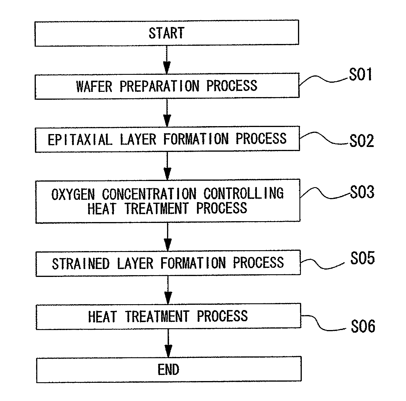
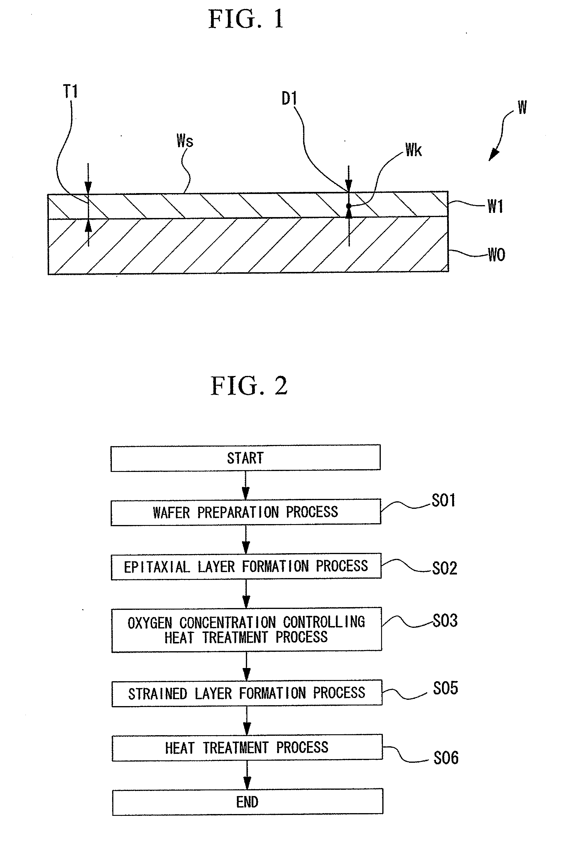
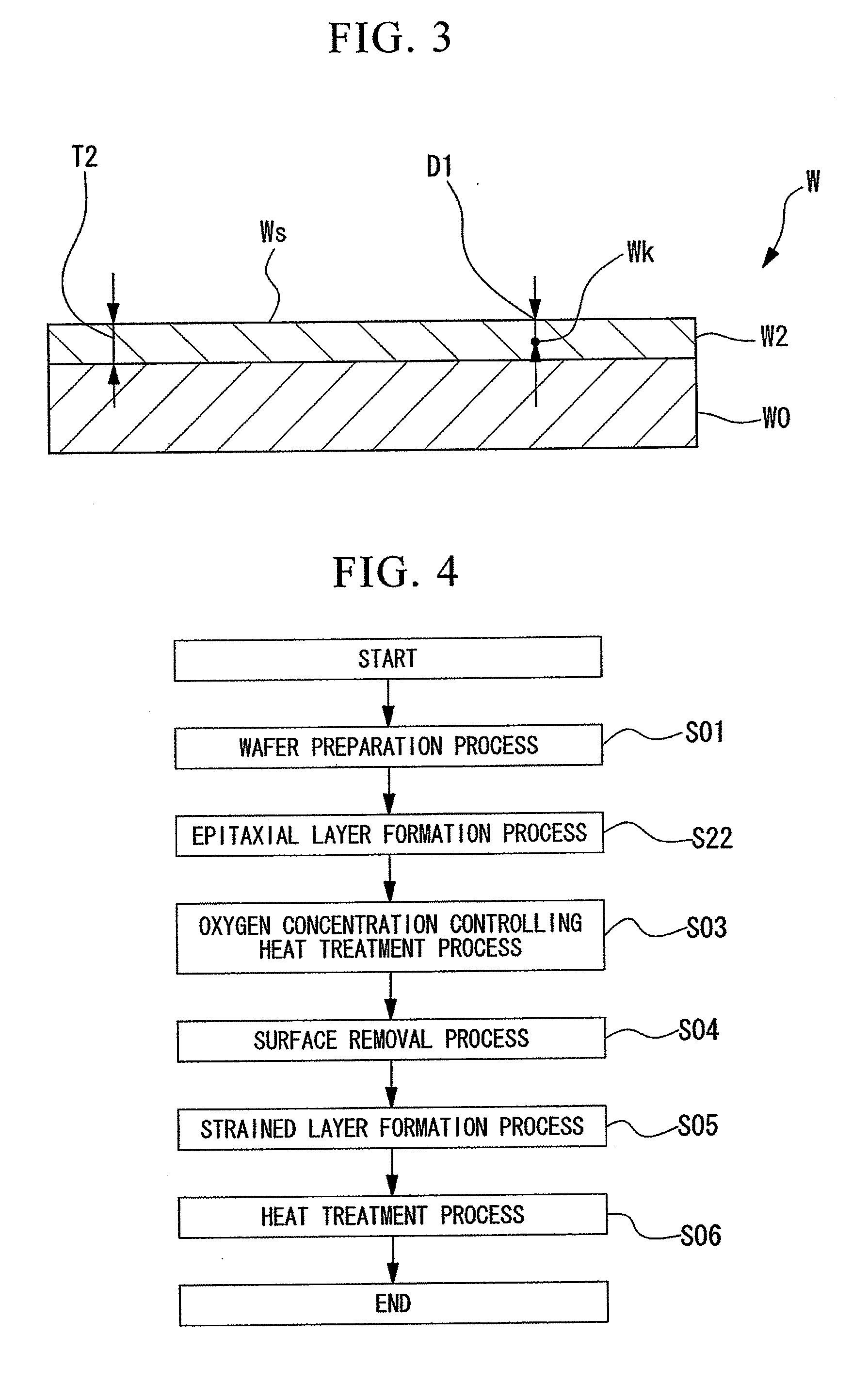
[0096]In Example 1, an Si layer having a predetermined thickness was epitaxially grown on a wafer sliced from a CZ single-crystalline wafer having a diameter of 300 mm and mirror-finished. In Examples 2 to 6, a heat treatment was performed for the same sample as that of Example 1 at 1,000° C. / 0.5 hrs under an Ar atmosphere using an upright furnace. In Examples 7 to 12, a heat treatment was performed at 1,150° C. / 30 sec under an Ar atmosphere using an RTA process furnace. Then, the wafer obtained through the heat treatment was ground from the surface side to produce samples by a predetermined thickness. The specifications of the samples are shown in Table 1 as follows.

TABLE 1Substrate OxygenEpi LayerGrindingSurface OxygenConcentrationThicknessThicknessConcentrationAmount of(E17atoms / cc)(μm)Heat Treatment(μm)(E17atoms / cc)DislocationExample 113.22N / AN / AUndetectableCExample 213.121000° C. / 0.5 hr0.31.2BExample 313.221000° C. / 0.5 hr13.3AExample 413.241000° C. / 0.5 hr0.3UndetectableCExample...

example 2

[0103]In Example 2, an Si layer having a predetermined thickness was epitaxially grown on a wafer sliced from a CZ single-crystalline wafer having a diameter of 300 mm and mirror-finished. The thickness of the grown epitaxial layer was 4 μm. Then, various kinds of heat treatments were performed. The heat treatment was performed in an RTA furnace under an oxidizing atmosphere if the treatment time is 180 sec or less. Meanwhile, the heat treatment was performed in an upright furnace under a mixture gas atmosphere (N2 and O2 (O2=10%)) if the treatment time is 180 sec or more. After the heat treatment, the generated oxide film was removed using a diluted HF solution, and a stress loading test was performed in a way similar to Example 1. The result is shown in FIG. 9.

[0104]According to the result, it is understood that the oxygen concentration of the epitaxial layer becomes high because the surface of the epitaxial layer is oxidized under an oxidizing atmosphere, the oxygen is inwardly d...


PUM


Abstract

A method of manufacturing an epitaxial wafer, including a silicon substrate having a surface sliced from single-crystalline silicon and a silicon epitaxial layer deposited on the surface of the silicon substrate, includes an oxygen concentration controlling heat treatment process in which a heat treatment of the epitaxial layer is performed under a non-oxidizing atmosphere after the epitaxial growth such that an oxygen concentration of the surface of the silicon epitaxial layer is set to 1.0×10¹⁷ to 12×1017 atoms/cm3 (ASTM F-121, 1979).

Description

BACKGROUND OF THE INVENTION[0001]1. Field of the Invention[0002]The invention relates to an epitaxial wafer and a method of manufacturing the same, and particularly, to technology suitable for an epitaxial wafer used in a process of forming a strained layer to improve a device characteristic.[0003]Priority is claimed on Japanese Patent Application No. 2008-318897, filed Dec. 15, 2008, the content of which is incorporated herein by reference.[0004]2. Description of the Related Art[0005]As silicon devices become more and more miniaturized, the vicinity of the wafer surface which is the active layer of the device is often strained to improve device characteristics.[0006]For example, a strained silicon wafer obtained by epitaxially growing a SiGe layer on a single-crystalline silicon wafer and epitaxially growing a strained silicon layer on the SiGe layer, a wafer obtained by changing the wafer from a SiGe layer to a nitriding of the surface, or a silicon-on-insulator (SOI) wafer have b...

Claims


Application Information

Patent Timeline
IPC IPC(8): H01L21/3205
CPCH01L21/02381H01L21/0245H01L29/7847H01L21/02658H01L21/3225H01L21/02532H01L29/0847H01L29/1608H01L29/161H01L29/165H01L29/66636H01L29/7843H01L29/7848
Inventor ONO, TOSHIAKIHOSHINO, YUMI
Owner SUMCO CORP
Why Eureka
Try Eureka