Preparation method of nanocrystals coated with metal-surfactant layers

a technology of metal-surfactant layers and nanocrystals, which is applied in the field of preparation of nanocrystals coated with metal-surfactant layers, can solve the problems of surface defects, affecting the luminescence efficiency of semiconductor nanocrystals, and affecting the performance of nanocrystals

Active Publication Date: 2010-06-24
SAMSUNG ELECTRONICS CO LTD
View PDF13 Cites 19 Cited by
  • Summary
  • Abstract
  • Description
  • Claims
  • Application Information

AI Technical Summary

Benefits of technology

[0008]Disclosed herein is a method for preparing nanocrystals, which includes synthesizing colloidal semiconductor nanocrystal cores; and adding a metal salt to the colloidal semiconductor nanocrystal cores and heating the mixture while maintaining the reaction temperature constant; etching the surfaces of the semiconductor nanocrystal cores to form etched surface portions of the semiconductor nanocrystal cores; and forming metal-surfactant layers derived from the metal salt as shells on the etched surface portions of the semiconductor nanocrystal cores.

Problems solved by technology

However, since the surfaces of semiconductor nanocrystals are prone to oxidation, surface defects are likely to be caused.
As a result, the luminescence efficiency of the semiconductor nanocrystals is liable to deteriorate and the core-shell structure of the semiconductor nanocrystals is destroyed.
However, etchants (e.g., HF) remove large amounts of organic materials present on the surfaces of nanocrystals rather than defects, making the nanocrystals unstable.

Method used


Image

  • Preparation method of nanocrystals coated with metal-surfactant layers
  • Preparation method of nanocrystals coated with metal-surfactant layers
  • Preparation method of nanocrystals coated with metal-surfactant layers

Examples


example 1

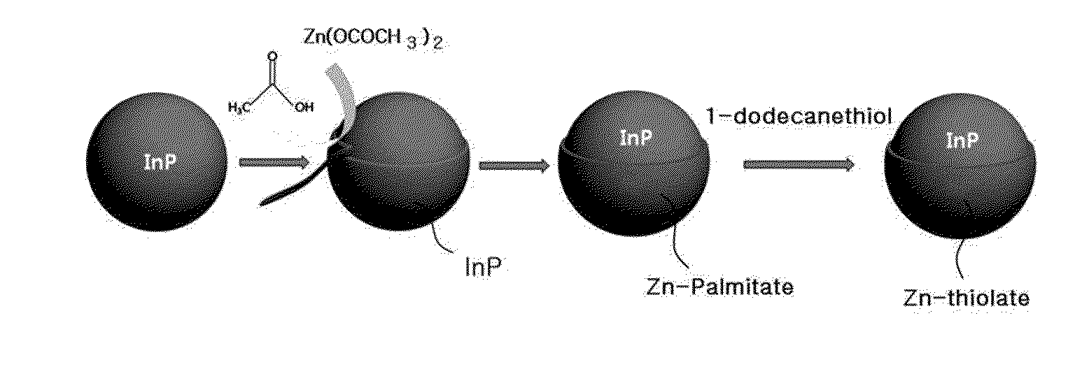
Preparation of InP / Zn-Palmitate Nanocrystals Emitting Light at 520 nm

[0054]Indium acetate (0.04 millimolar (“mmol”), 11.34 milligrams (“mg”)) is added to a mixture of palmitic acid (0.12 mmol, 30.77 mg) and octadecene (2 milliliters (“mL”)), heated to 110° C., and maintained under vacuum for 1.5 hours to remove a small amount of water. The resulting mixture is heated to 300° C. under an argon atmosphere, and then a solution of trimethylsilyl-3-phosphine (0.02 mmol, 5 mg) in octadecene (3 mL) is added thereto. The reaction mixture is rapidly cooled to room temperature to give colloidal InP nanocrystals.

[0055]Zinc acetate (0.1 mmol, 18.35 mg) is added to the colloidal InP nanocrystals at room temperature and heated to 230° C. The growth of the InP nanocrystals is observed at intervals of 1 to 2 hours until the PL intensity increases. The mixture is cooled to room temperature to give colloidal InP core / Zn-palmitate shell nanocrystals. Then, the colloidal InP / Zn-palmitate nanocrystals a...

example 2

Preparation of InP / Zn-Palmitate Nanocrystals Emitting Light at 580 nm

[0056]0.12 mmol (34.034 mg) of indium acetate is added to a mixture of 0.36 mmol (92.31 mg) of palmitic acid and 2 mL of octadecene, heated to 110° C., and maintained under vacuum for 1.5 hours to remove a small amount of water. The resulting mixture is heated to 300° C. under an argon atmosphere, and then a solution of 0.06 mmol (15 mg) of trimethylsilyl-3-phosphine in 1 mL of octadecene is added thereto. The reaction mixture is heated to 270° C., maintained at 270° C. for 30 minutes, and rapidly cooled to room temperature to give colloidal InP nanocrystals. 0.30 mmol (55.04 mg) of zinc acetate is added to the colloidal InP nanocrystals at room temperature and heated to 230° C. The growth of the InP nanocrystals is observed at intervals of 3 to 4 hours until the PL intensity increases. The mixture is cooled to room temperature to give colloidal InP core / Zn-palmitate shell nanocrystals. Then, the colloidal InP / Zn-p...

example 3

Preparation of InP / Zn-Palmitate Nanocrystals Emitting Light at 600 nm

[0057]InP / Zn-palmitate nanocrystals are prepared in the same manner as in Example 2, except that 0.16 mmol (46.71 mg) of indium acetate is added to a mixture of 0.48 mmol (122.94 mg) of palmitic acid and 8 mL of octadecene, and 0.08 mmol (20 mg) of trimethylsilyl-3-phosphine is dissolved in 1 mL of octadecene. FIG. 5 shows that the InP / Zn-palmitate nanocrystals emit light at 600 nm.


PUM

PropertyMeasurementUnit
reaction temperatureaaaaaaaaaa

Abstract

A method for preparing nanocrystals is disclosed. The method includes synthesizing colloidal semiconductor nanocrystal cores, and adding a metal salt to the colloidal semiconductor nanocrystal cores and heating the mixture while maintaining the reaction temperature constant. During the reaction, the surfaces of the semiconductor nanocrystal cores are etched (‘in-situ etching’) and metal-surfactant layers are formed on the etched surface portions of the semiconductor nanocrystal cores. The metal-surfactant layers are derived from the metal salt. Nanocrystals prepared by the method have minimal surface defects and exhibit high luminescence efficiency and good stability.

Description

CROSS-REFERENCE TO RELATED APPLICATION[0001]This application claims priority to Korean Patent Application No. 10-2008-130499, filed on Dec. 19, 2008, and all the benefits accruing therefrom under 35 U.S.C. §119, the contents of which in its entirety are herein incorporated by reference.BACKGROUND[0002]1. Field[0003]The disclosure is directed to a method for preparing nanocrystals coated with metal-surfactant layers. More specifically, the method is directed to the preparation of nanocrystals with minimal surface defects, high luminescence efficiency and good stability.[0004]2. Description of the Related Art[0005]A semiconductor nanocrystal, also called a “quantum dot,” is a crystalline semiconductor material of the size of a few nanometers and consists of several hundred to several thousand atoms. A semiconductor nanocrystal has a large surface area per unit volume and exhibits a variety of effects (e.g., quantum confinement) that are different from those exhibited by a bulk materia...

Claims


Application Information

Patent Timeline
Patent Type & Authority Applications(United States)
IPC IPC(8): B32B5/16H01L21/30
CPCB82Y20/00B82Y30/00Y10T428/2991H01L51/5012H05B33/14C09K11/70H10K50/11B82B1/00B82B3/00
Inventor JANG, EUN JOOKIM, SANG WOOK
Owner SAMSUNG ELECTRONICS CO LTD
Why Eureka
Try Eureka