Mounting table structure and heat treatment apparatus

a technology of heat treatment apparatus and mounting table, which is applied in electrical apparatus, coatings, semiconductor/solid-state device manufacturing, etc., can solve the problems of metal contamination, damage to the mounting table, and reduction in production yield, so as to improve the reproducibility of heat treatment and the in-plane temperature uniformity of the target obj

a technology of heat treatment apparatus and mounting table, which is applied in electrical apparatus, coatings, semiconductor/solid-state device manufacturing, etc., can solve the problems of metal contamination, damage to the mounting table, and reduction in production yield, so as to improve the reproducibility of heat treatment and the in-plane temperature uniformity of the target obj

US20100163183A1Inactive Publication Date: 2010-07-01TOKYO ELECTRON LTD

Image

  • Mounting table structure and heat treatment apparatus
  • Mounting table structure and heat treatment apparatus
  • Mounting table structure and heat treatment apparatus

Examples


Embodiment Construction

[0031]Hereinafter, a mounting table structure and a heat treatment apparatus in accordance with embodiments of the present invention will be described with reference to the accompanying drawings.

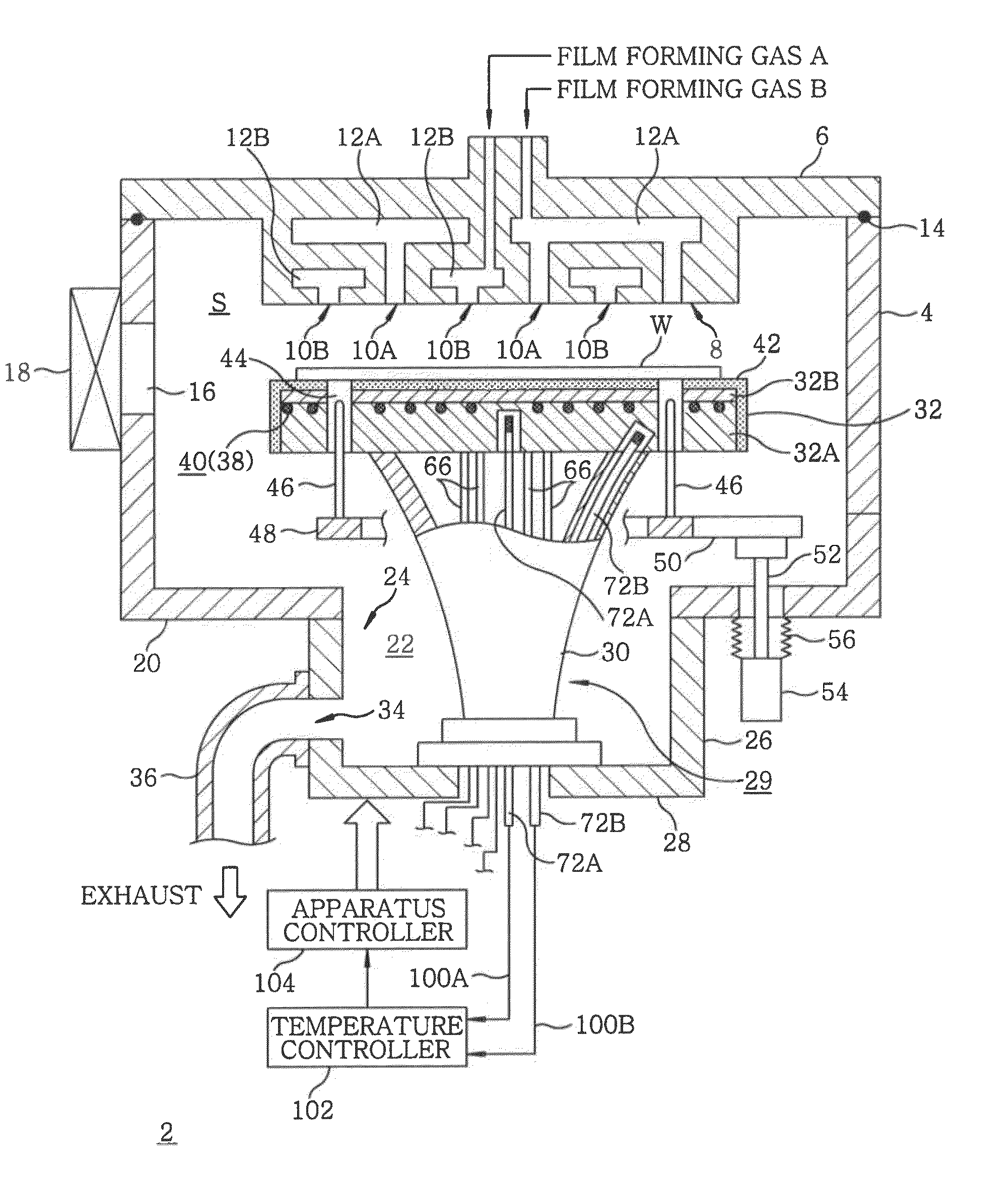
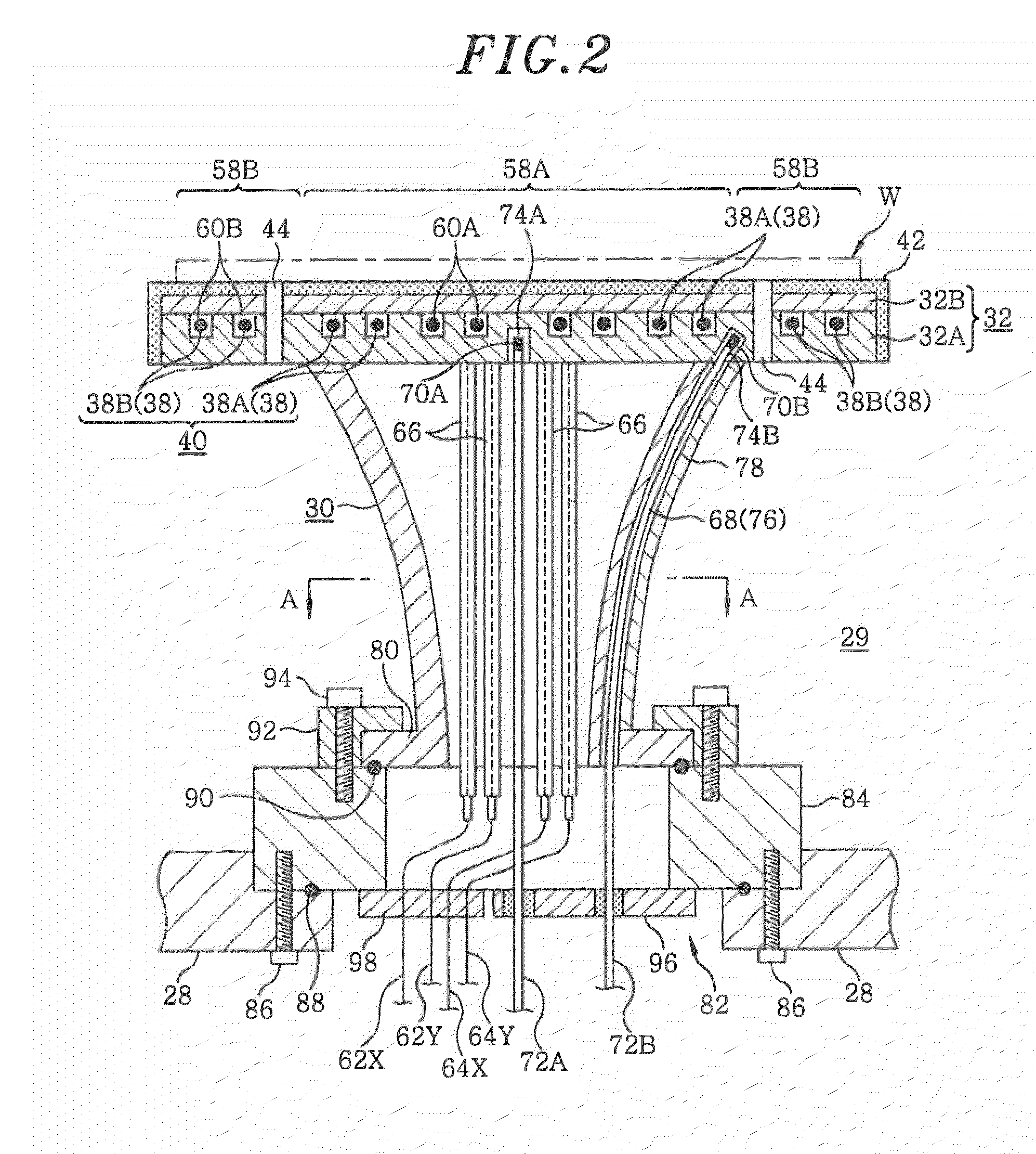
[0032]FIG. 1 is a longitudinal cross sectional view of a heat treatment apparatus in accordance with an embodiment of the present invention. In this embodiment, a film forming apparatus is described as an example of the heat treatment apparatus. FIG. 2 is an enlarged longitudinal cross sectional view showing a mounting table structure of FIG. 1. FIG. 3 illustrates a plan view of a mounting table main body in which resistance heaters are arranged. FIG. 4 is a cross sectional view of a column, which is taken along line A-A of FIG. 2. FIGS. 5A to 5C illustrate a procedure for forming an insertion passageway at a sidewall of the column. FIG. 6 illustrates a state when the column is fitted on a mounting table.

[0033]As shown in FIG. 1, a heat treatment apparatus 2 includes a processing chamber 4 m...


PUM

PropertyMeasurementUnit
temperatureaaaaaaaaaa
structureaaaaaaaaaa
temperatureaaaaaaaaaa

Abstract

A mounting table structure includes a mounting table provided with a heating unit having heaters respectively arranged in concentrically divided heating zones and on which an object to be heat-treated is placed, a temperature measurement units respectively arranged in the heating zones, and a hollow column for supporting the mounting table in an upstanding state. The diameter of the column is gradually expanded from its bottom to its top, and the upper end of the column is bonded to the bottom surface of the mounting table. A measurement unit main body of each temperature measurement unit is inserted into the hollow column and an insertion passageway provided at a sidewall of the column.

Description

[0001]This application is a Continuation Application of PCT International Application No. PCT / JP2008 / 061568 filed on Jun. 25, 2008, which designated the United States.FIELD OF THE INVENTION[0002]The present invention relates to a heat treatment apparatus for treating a target object such as a semiconductor wafer and a mounting table structure used in the heat treatment apparatus.BACKGROUND OF THE INVENTION[0003]Generally, in manufacturing semiconductor integrated circuits, various single-wafer processes such as a film forming process, an etching process, a heat treatment, a modification process and a crystallization process are repeatedly carried out on a target object such as a semiconductor wafer to form desired integrated circuits. In such processes, processing gases required for the corresponding processes, e.g., a film forming gas for the film forming process, an ozone gas or the like for the modification process, and an O2 gas, a nonreactive gas such as N2 gas or the like for ...

Claims


Application Information

Patent Timeline
01 Jul 2010
Publication
US20100163183A1
IPC
C23F1/08; B05C11/00
CPC
H01L21/67109; H01L21/67248; H01L21/68792; H01L21/324; H01L21/683
Inventors
TANAKA, SUMI; KAWASAKI, HIROO