Organic electroluminescent device

Active Publication Date: 2010-07-01
IDEMITSU KOSAN CO LTD
View PDF7 Cites 16 Cited by
  • Summary
  • Abstract
  • Description
  • Claims
  • Application Information

AI Technical Summary

Benefits of technology

vention can provide an organic EL device having an improved luminous efficiency and a prolonged lifetime (under conditions at room temperature and at high temperatures).
r, the invention can provide

Problems solved by technology

However, at high temperatures, the carrier balance significantly varies from that at room temperature due to heat, thus, a clear solution of the problem at high temperatures cannot be ea

Method used


Image

  • Organic electroluminescent device
  • Organic electroluminescent device
  • Organic electroluminescent device

Examples


Example

Example 1

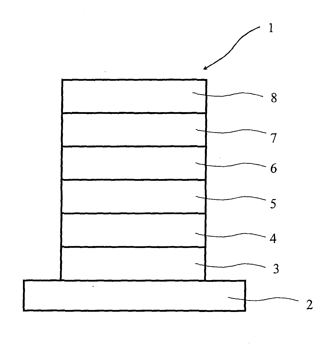
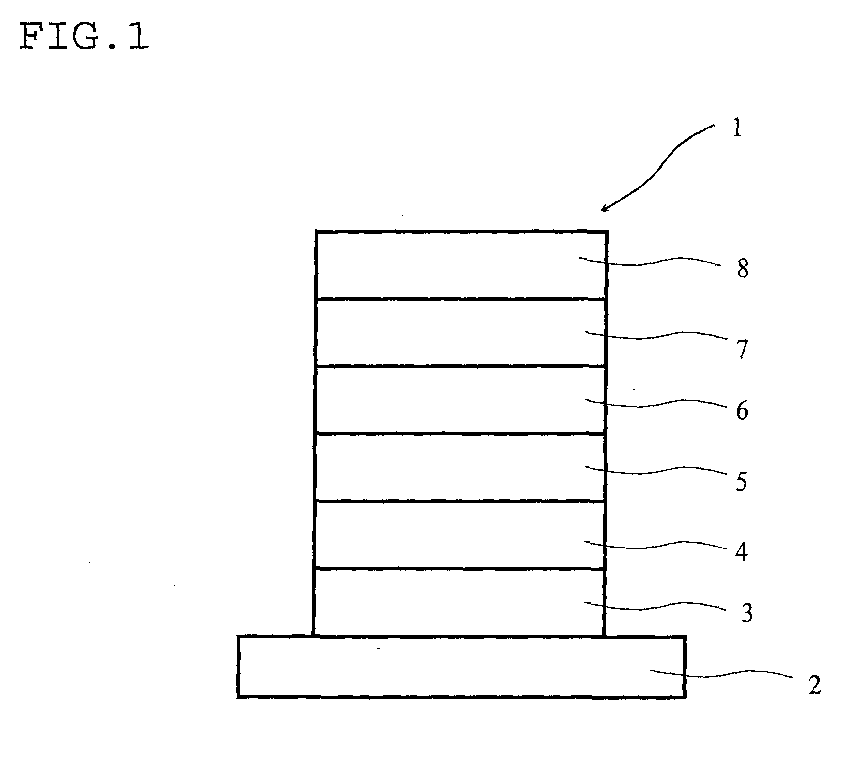
[0342]A glass substrate (made by Geomatic Co.) measuring 25 mm by 75 mm by 0.7 mm-thickness with an ITO transparent electrode was subjected to ultrasonic wave cleaning in isopropyl alcohol for five minutes and then to UV ozone cleaning for thirty minutes. This glass substrate with the transparent electrode line was set on a vapor deposition apparatus, and following compound (HT1) was deposited in a thickness of 50 nm on the surface of a side on which the transparent electrode line was formed so as to cover the transparent electrode. The HT1 layer functions as a hole injecting / transporting layer. As a host of the emitting layer, following compound (H2) was formed in a thickness of 40 nm by a resistance heating deposition. At the same time, as a phosphorescent dopant, the following compound (D1) was deposited with a mass ratio to the compound (H2) of 10%. This layer functions as an emitting layer. Next, the following compound (H3) forming an electron-injecting controlling lay...

Example

Example 2

[0344]An organic EL device was prepared in the same manner as Example 1 expect for using the following compound (H4) as the electron-injecting controlling layer.

Example

Example 3

[0345]An organic EL device was prepared in the same manner as Example 1 expect for using the following compound (H5) as the electron-injecting controlling layer.


PUM


Abstract

An organic electroluminescent device including an emitting layer, an electron-injecting controlling layer and an electron-transporting layer between an anode and a cathode in sequential order from the anode, bonding one to another, the emitting layer including a host material and a dopant, the ionization potential (Ips) of the main material forming the electron-injecting controlling layer and the ionization potential (Iph) of the host material of the emitting layer satisfying the following relationship (i), the electron mobility of the electron-transporting material forming the electron-transporting layer being 10−5 cm2/Vs or more at the electric field intensity of 400 to 500 (V/cm)1/2, and the affinity level (Af1) of the host material of the emitting layer, the affinity level (Af2) of the main material forming the electron-injecting controlling layer, and the affinity level (Af3) of the electron-transporting material forming the electron-transporting layer satisfying the following relationships (ii) and (iii).
0.5 eV>Ips−Iph≧0 eV  (i)
Af2−Af1>0 eV  (ii)
Af3−Af2>0.2 eV  (iii)

Description

TECHNICAL FIELD[0001]The invention relates to an organic electroluminescence device, particularly to an organic electroluminescence device having a prolonged lifetime even when it is driven at high temperatures.BACKGROUND ART[0002]An organic electroluminescence device (hereinafter the term “electroluminescence” is often abbreviated as “EL”) is a self-emission device utilizing the principle that a fluorescent compound emits light by the recombination energy of holes injected from an anode and electrons injected from a cathode when an electric field is impressed. Since C. W. Tang et al. of Eastman Kodak Co. reported a low-voltage driven organic EL device in the form of a stacked type device (Non-patent Document 1, or the like), studies on organic EL devices wherein organic materials are used as the constituent materials have actively been conducted. Tang et al. used tris(8-hydroxyquinolinol aluminum) (hereinafter referred to as Alq3) for the emitting layer and a triphenyl diamine deri...

Claims


Application Information

Patent Timeline
IPC IPC(8): H01L51/54
CPCH10K85/625H10K85/6572H10K50/11H10K2101/10H10K2101/30H10K50/171H10K50/17
Inventor OGIWARA, TOSHINARINISHIMURA, KAZUKIIWAKUMA, TOSHIHIRO
Owner IDEMITSU KOSAN CO LTD
Why Eureka
Try Eureka