

Micromechanical component and corresponding production method
- Summary
- Abstract
- Description
- Claims
- Application Information
AI Technical Summary
Benefits of technology
Problems solved by technology
Method used
Image

Examples
Embodiment Construction
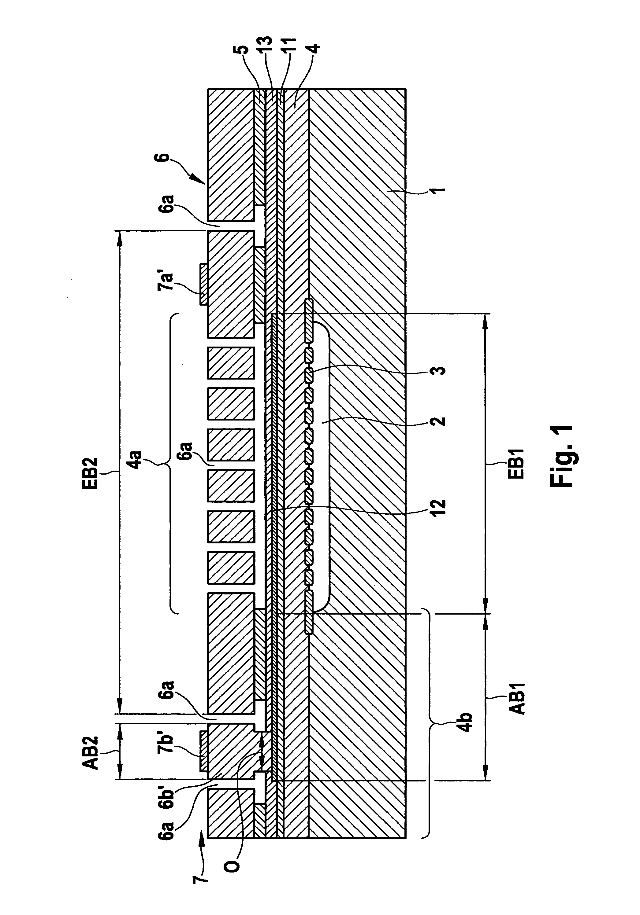
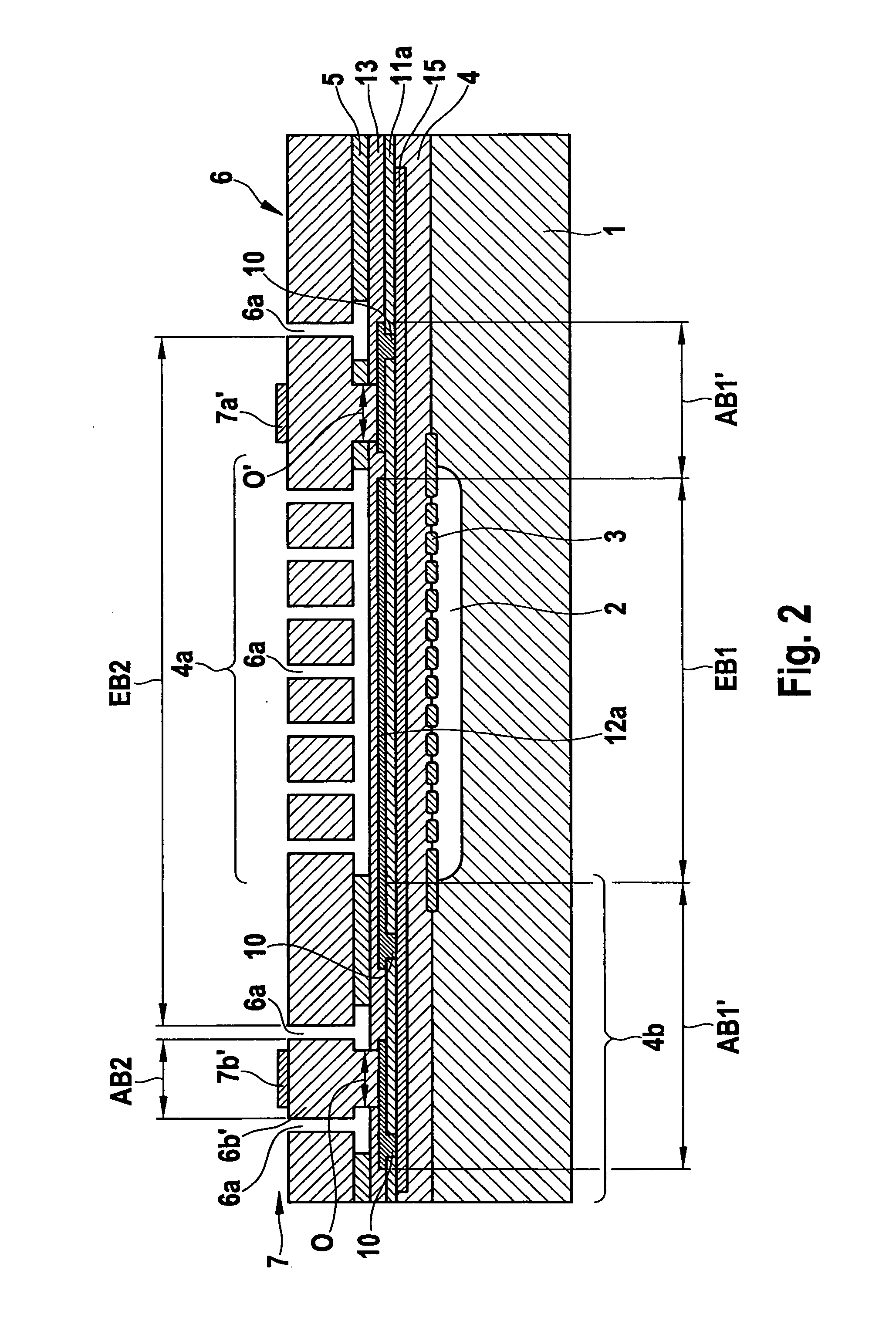
[0023]In the figures, like reference numerals designate like or functionally equivalent components.
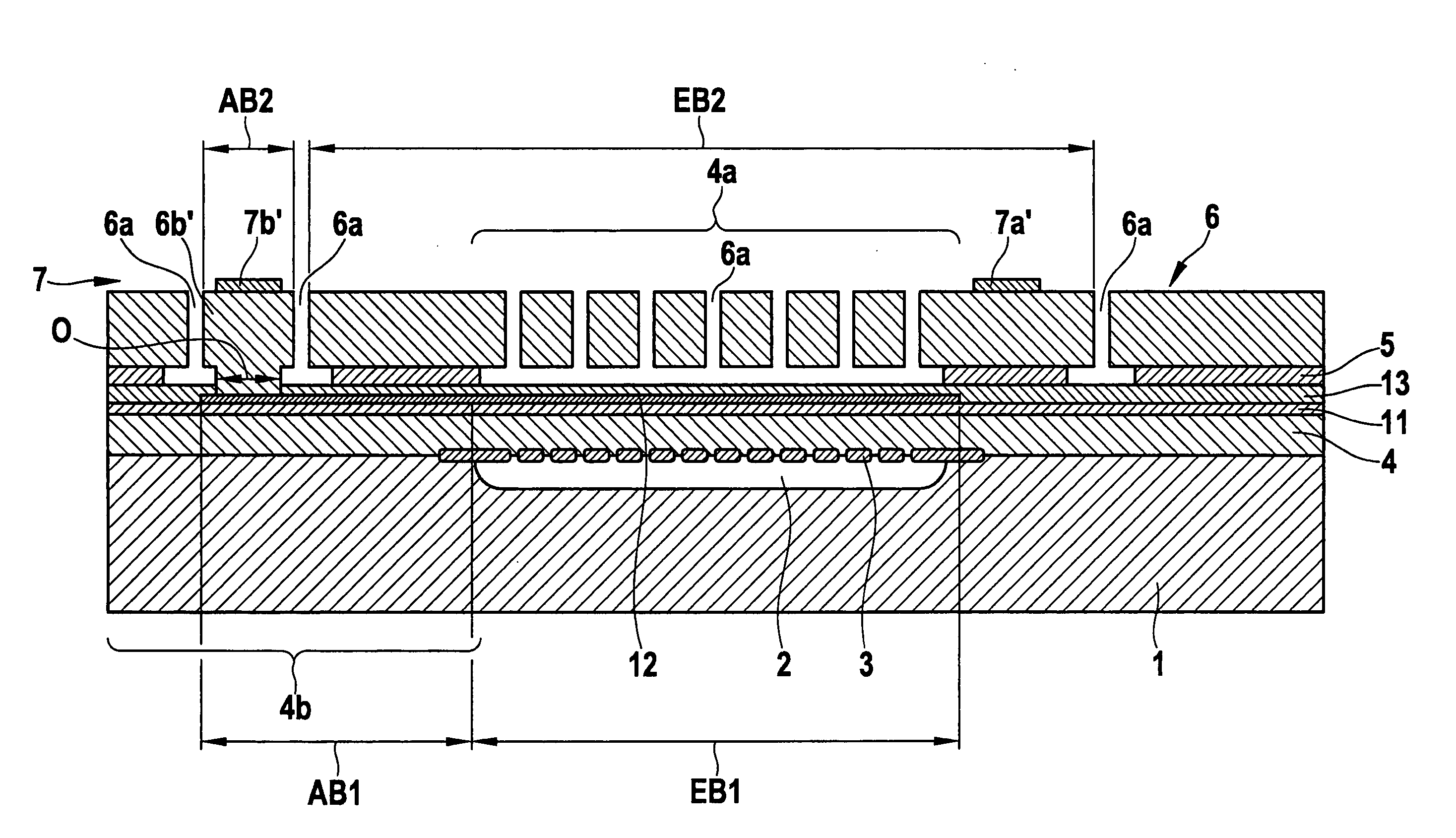
[0024]FIG. 1 shows a schematic sectional view of a capacitive pressure sensor to explain the structure of a micromechanical component in the form of a capacitive pressure sensor according to a first specific embodiment of the present invention.
[0025]In FIG. 1, reference numeral 1 labels a conductive silicon substrate having a first conductive layer 4 of monocrystalline silicon, which is provided above substrate 1 and which forms, above a cavity 2 provided in substrate 1, an elastically deflectable diaphragm region 4a and an adjacent peripheral region 4b. As a result of the production process (see above regarding FIG. 6), a monocrystalline silicon lattice 3 is provided above cavity 2 between substrate 1 and first conductive layer 4, which also allows for a conductive layer 4 growing in a monocrystalline manner in diaphragm region 4a. A first insulation layer 11 of silicon oxide is provi...
PUM
 Abstract
Description
Claims
Application Information