Display driver and display driving method

a technology of display driver and display, applied in the field of display driver, can solve the problems of increasing the circuit scale and affecting the effect of reducing the fluctuation of the holding potential

Active Publication Date: 2010-07-01
RENESAS ELECTRONICS CORP
View PDF3 Cites 6 Cited by
  • Summary
  • Abstract
  • Description
  • Claims
  • Application Information

AI Technical Summary

Benefits of technology

[0006]Accordingly, an object of the present invention is to provide a display driver, which can reduce a holding potential fluctuation of a data line without adding any new circuit and without depending on a display pattern.
[0007]As mentioned above, in order to reduce the fluctuation of the holding potential of the data line in the floating state, it is effective to reduce the potential difference between the pre-charge voltage and the original data voltage. In other words, the fluctuation of the holding potential can be dissolved if the pre-charge voltage can be made equal to the original data voltage. Paying attention to this point, in the display driver according to the present invention, a pre-charge voltage equal to an original data voltage is applied to data lines in one block in a time-sharing manner in a period P, and the original data voltage is applied again in a time-sharing manner in the subsequent period D. Accordingly, paying attention to a certain data line, the same data voltage is applied twice within one scanning period. Therefore, the pre-charge voltage and the original data voltage become equal, and it is possible to dissolve the fluctuation of the holding potential.
[0008]According to the present invention, since it is possible to make the pre-charge voltage equal to the original data voltage in all the data lines only by changing the output operation of the data voltage in the time-sharing drive, it is possible to provide the display driver which can reduce the holding potential fluctuation of the data line without newly adding the circuit and without depending on the display pattern.

Problems solved by technology

However, in the method described in Japanese Patent Application Laid-Open Publication No. 2004-191544 mentioned above, since it is necessary to newly add a circuit for calculating the average value of the data voltages, there is a problem that a circuit scale is increased.
Further, since such a case may occur where a data voltage largely deviated from the average value is applied depending on a display data, there is a problem that a display pattern dependency affects the effect of reducing the holding potential fluctuation.

Method used


Image

  • Display driver and display driving method
  • Display driver and display driving method
  • Display driver and display driving method

Examples


first embodiment

[0022]A configuration and an operation of a display driver according to a first embodiment of the present invention will be described below with reference to FIG. 1 and FIG. 2.

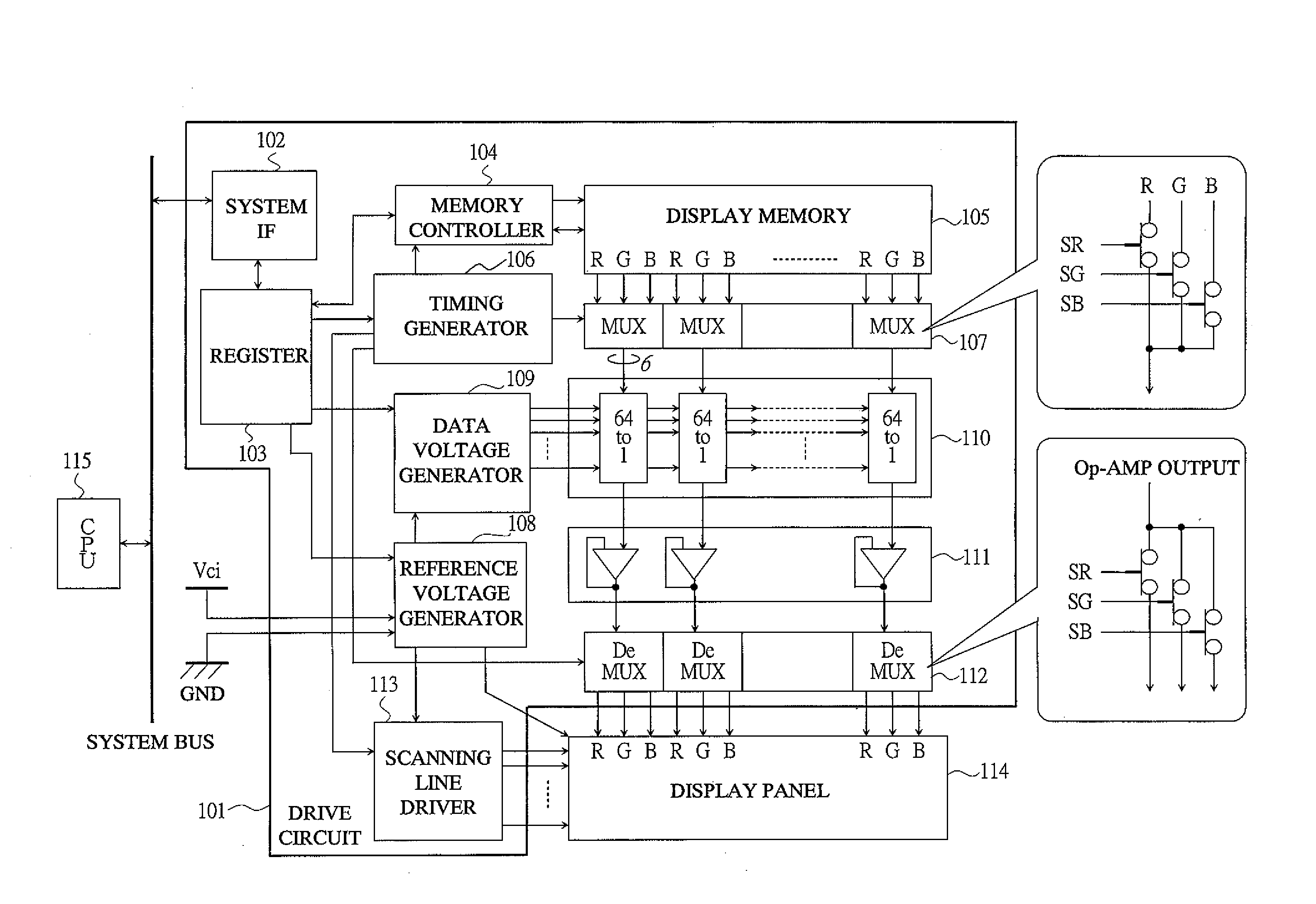
[0023]First, FIG. 1 shows a block configuration of a display driver according to a first embodiment of the present invention. In FIG. 1, a reference numeral 101 denotes a drive circuit, 102 denotes a system interface (IF), 103 denotes a register, 104 denotes a memory controller, 105 denotes a display memory, 106 denotes a timing generator, 107 denotes a multiplexer (MUX), 108 denotes a reference voltage generator, 109 denotes a data voltage generator, 110 denotes a data voltage selector (64 to 1), 111 denotes an operational amplifier (Op-AMP), 112 denotes a demultiplexer (DeMUX), 113 denotes a scanning line driver, 114 denotes a display panel, and 115 denotes a CPU.

[0024]The drive circuit 101 is a so-called display memory built-in type controller driver, and it includes achieving means according to the present...

second embodiment

[0044]Next, a configuration and an operation of a display driver according to a second embodiment of the present invention will be described with reference to FIG. 3 to FIG. 5.

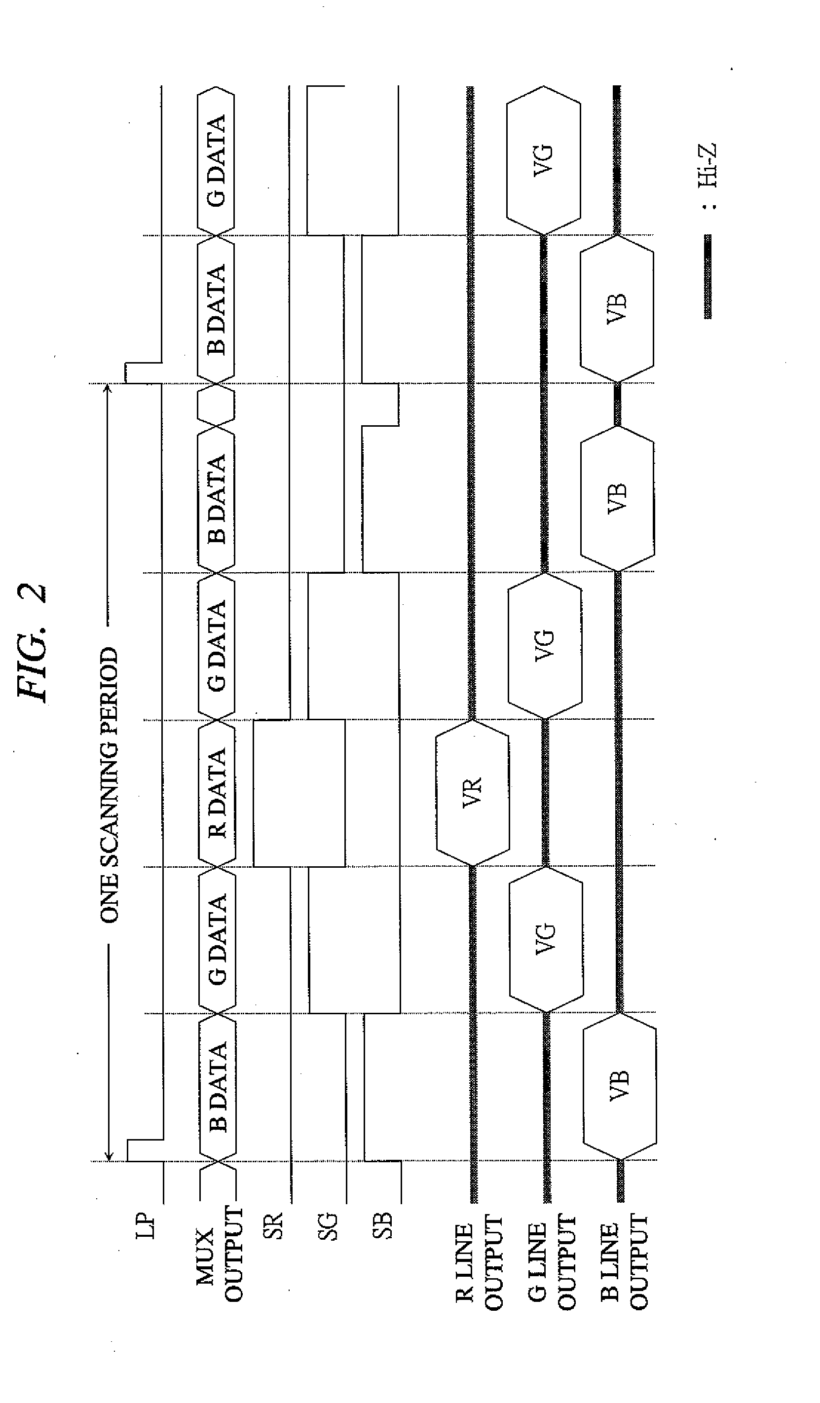
[0045]As described above, in the first embodiment of the present invention, the method in which the data voltage is applied in the order of B→G→R→G→B has been described. In this embodiment, the B line is driven just after starting the one scanning period, and since the outputs to the G line and the R line become high impedance in this period, the potential applied in the previous scanning period is held. In this case, assuming a so-called Vcom alternating current drive in which the voltage Vcom is alternated in each one scanning period, since the Vcom electrode and the data line are capacity-coupled to each other, the holding voltage of the data line transits in conjunction with the transition of the voltage Vcom, and the holding potential after the transition exceeds the amplitude range of the data voltage in...

third embodiment

[0053]Next, a configuration and an operation of a display driver according to a third embodiment of the present invention will be described with reference to FIG. 6 to FIG. 8.

[0054]In the third embodiment of the present invention, two types of pre-charge levels are provided for the pre-charge level of the fixed potential described in the second embodiment of the present invention so as to further reduce the potential difference between before and after the first data voltage is applied, thereby achieving the further improvement of the operation margin in the time-sharing drive. In this embodiment, two types of pre-charge levels are the power supply voltages Vci and GND, and the pre-charge is controlled by using the display data.

[0055]FIG. 6 shows a block configuration of a display driver according to the third embodiment of the present invention. In FIG. 6, a reference numeral 301 denotes a drive circuit, and 302 denotes a demultiplexer. Since the other blocks are the same as the co...


PUM


Abstract

In a display driver, one scanning period is divided into a period P and a subsequent period D. In the period P, a pre-charge voltage equal to an original data voltage is applied in a time-sharing manner to data lines in one block, and in the period D after the period P, the original data voltage is applied again.

Description

CROSS-REFERENCE TO RELATED APPLICATION[0001]This application is a continuation application of U.S. Ser. No. 11 / 286,429, filed Nov. 25, 2005, and which application claims priority from Japanese Patent Application No. JP 2005-86878 filed on Mar. 24, 2005, the contents of which are hereby incorporated by reference into this application.TECHNICAL FIELD OF THE INVENTION[0002]The present invention relates to a display driver for an active matrix display using a TFT liquid crystal or the like. More particularly, it relates to a technology effectively applied to a driving method and a drive circuit which can suppress a fluctuation of data voltage held in a data line, in a drive system in which the data voltage is outputted in a time-sharing manner in one horizontal period.BACKGROUND OF THE INVENTION[0003]In general, in the active matrix display in which a plurality of scanning lines and a plurality of data lines are arranged in a matrix shape, a scanning voltage showing a selected state is ...

Claims


Application Information

Patent Timeline
Patent Type & Authority Applications(United States)
IPC IPC(8): G09G5/10G09G3/34
CPCG09G2310/0248G09G2310/027G09G2310/0297G09G2310/08G09G2320/0209G09G3/20G09G3/2003G09G3/3688G09G2310/0235G09G3/36
Inventor KUDO, YASUYUKIAKAI, AKIHITOSAKAMAKI, GORO
Owner RENESAS ELECTRONICS CORP
Why Eureka
Try Eureka