Memory module

a memory module and memory technology, applied in the field of memory modules, can solve the problems of limiting the access speed of those subsystems, limiting the ability of those memory systems to provide improved operating speed, and limiting the processing speed of computing devices

Inactive Publication Date: 2010-07-01
SEGARAM PARA KANAGASABAI
View PDF9 Cites 27 Cited by
  • Summary
  • Abstract
  • Description
  • Claims
  • Application Information

AI Technical Summary

Benefits of technology

[0012]We have found that with this memory architecture, it is possible to provide any memory module with much faster access speeds as well as a module that can operate with lower power between the memory modules, such as DIMM (Dual In-line Memory Module) modules, and the memory controller.
[0077]Nanostructure materials suitable for electrically connecting respective substrates may include a variety of materials including carbon nanotubes, nanowires, nanocoils and nanosprings. These materials may preferably be embedded in an insulating material to provide a structural support for the nanostructures. The nanostructures embedded in the insulating material may conveniently provide a sacer to retrain the substrates in a desired position.

Problems solved by technology

Computing sub systems often limit the processing speed of computing devices because of a variety of physical limitations which limits the access speed of those subsystems.
The physical limits of transistor technology as employed in the architecture used for the current generation of memory systems significantly limit the ability of those memory systems to provide improved operating speed.
In practice, the speed or performance of a computer is very often more limited by the capabilities of the high speed differential line between the memory and memory controller and the architecture of which rather than by the operating speed of the micro processor.
Approaches that have been employed to improve the speed of access to the memory in fully buffered memory differential line structures have been limited to the standard circuit traces / electrical connectors that are currently used as an integral part of the interconnection of the memory modules to the memory controller.
Because Advanced Memory Buffer (AMB) devices operate at high speed, high power, with large silicon areas and complex transceiver implementations the current approaches for improving the speed of access to the memory are limited.
This type of architecture, even when designed for high-speed memory module cards, places a number of physical limitations that limit the access speed to the memory.

Method used


Image

  • Memory module
  • Memory module
  • Memory module

Examples


Embodiment Construction

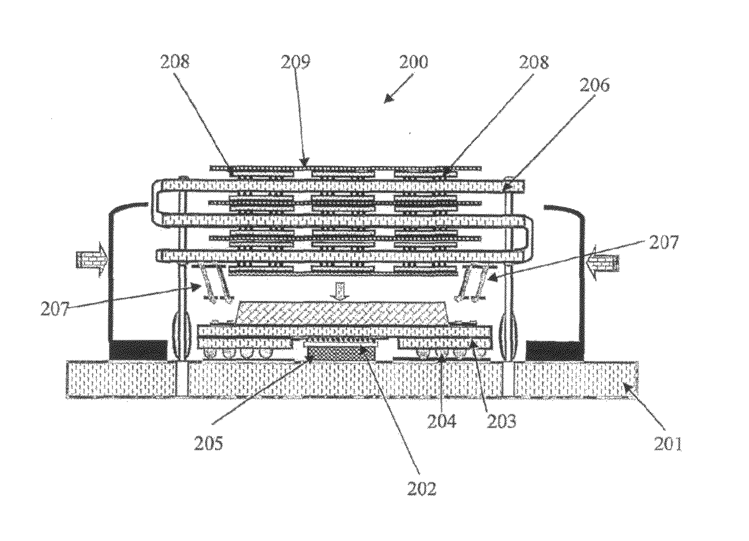
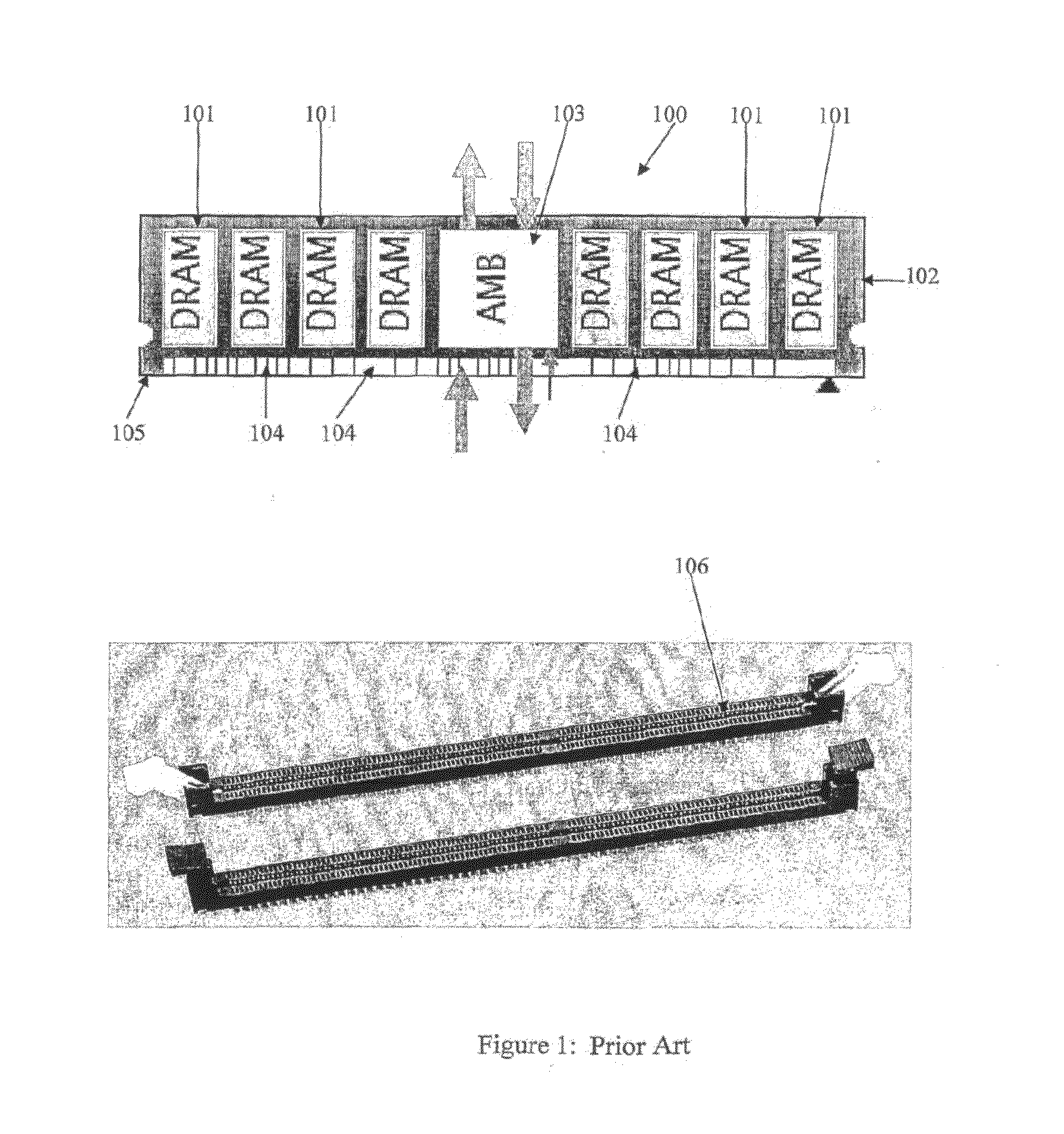
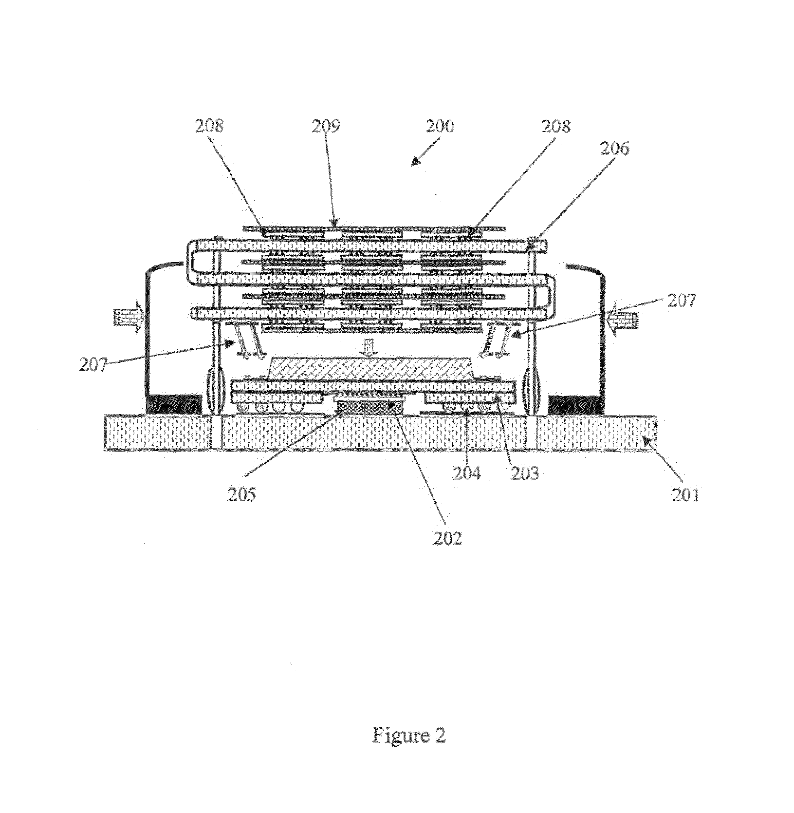
[0010]We have now found a memory architecture that provides for high access speed and low powered signalling between the memory module and the memory controller. According to a first aspect of the present invention, there is provided a sub system for a computing device comprising a plurality of chips mounted on a foldable substrate wherein the foldable substrate and the chips are layered by folding the substrate whereby the chips are disposed in at least one stacked configuration and wherein the sub system is adapted to be received on a host board.

[0011]In a preferred embodiment of the present invention the sub system is a memory module for a computing device. In this embodiment there is provided a memory module for a computing device comprising a plurality of memory chips mounted On a foldable substrate wherein the foldable substrate and the memory chips are layered by folding the substrate whereby the memory chips are disposed in at least one stacked configuration and wherein the ...


PUM


Abstract

A sub system for a computing device comprising a plurality of chips mounted on a foldable substrate wherein the foldable substrate and the chips are layered by folding the substrate whereby the chips are disposed in at least one stacked configuration and wherein the sub system is adapted to be received on a host board. In addition, removable connections using resilient and nanostructure based members.

Description

FIELD OF THE INVENTION[0001]The present invention relates to a sub system for computing devices. In particular, the present invention relates to the architecture of such sub systems. The present invention has particular application to memory modules but it will be appreciated that the invention will find other application to computing devices. In addition, the present invention relates to the removable connection of elements of a computing device.BACKGROUND OF THE INVENTION[0002]Computing sub systems often limit the processing speed of computing devices because of a variety of physical limitations which limits the access speed of those subsystems. The present invention will now be described with reference to the manufacture of computer memory, in particular memory modules. However it will be appreciated that the present invention will be applicable to other computing subsystems. For example, communication subsystems including an analog transceiver along with a number of digital devi...

Claims


Application Information

Patent Timeline
Patent Type & Authority Applications(United States)
IPC IPC(8): G06F1/16
CPCG06F1/185G11C5/02G11C5/04H01L23/5387H01L25/105H01L2924/3011H05K1/141H05K1/144H05K1/147H05K1/189H05K3/325H05K2201/0311H05K2201/042H05K2201/10386H05K2201/10515H05K2201/1053H05K2201/10674H05K2201/10734H05K2203/048H05K2203/1572H05K2203/167H01L2924/0002H01L2924/15311H01L2924/00
Inventor SEGARAM, PARA KANAGASABAI
Owner SEGARAM PARA KANAGASABAI
Why Eureka
Try Eureka