Method and Apparatus for Light Absorption and Charged Carrier Transport

a technology of which is applied in the field of method and apparatus for light absorption and charge carrier transport, can solve the problems of difficult to find or synthesize organic solar cells suitable materials, low efficiency still far below the theoretical limit, and sub>60/sub> is not a very strong absorber of light with wavelength longer than 530 nm

Inactive Publication Date: 2010-07-08
UNIV OF FLORIDA RES FOUNDATION INC
View PDF18 Cites 10 Cited by
  • Summary
  • Abstract
  • Description
  • Claims
  • Application Information

AI Technical Summary

Problems solved by technology

Therefore, it is unlikely that the use of binary compound semiconductors, which have fixed stoichiometry, will achieve the optimized band gap and the optimized electron affinity simultaneously.
However, such efficiencies are still far lower than the theoretical limits, and it is imperative to greatly improve the efficiency to make this technology suitable for large-scale commercial applications.
While some organic materials can have slightly longer exciton diffusion lengths, it is generally difficult to find or synthesize such materials that are suitable for organic solar cel

Method used


Image

  • Method and Apparatus for Light Absorption and Charged Carrier Transport
  • Method and Apparatus for Light Absorption and Charged Carrier Transport

Examples


Embodiment Construction

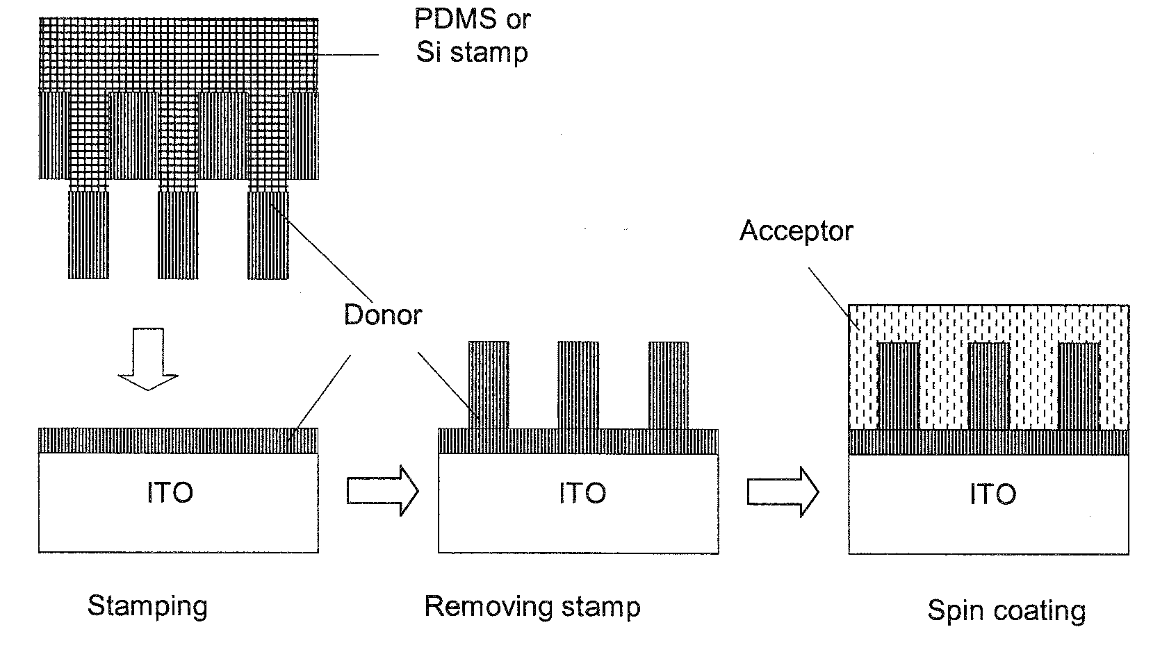
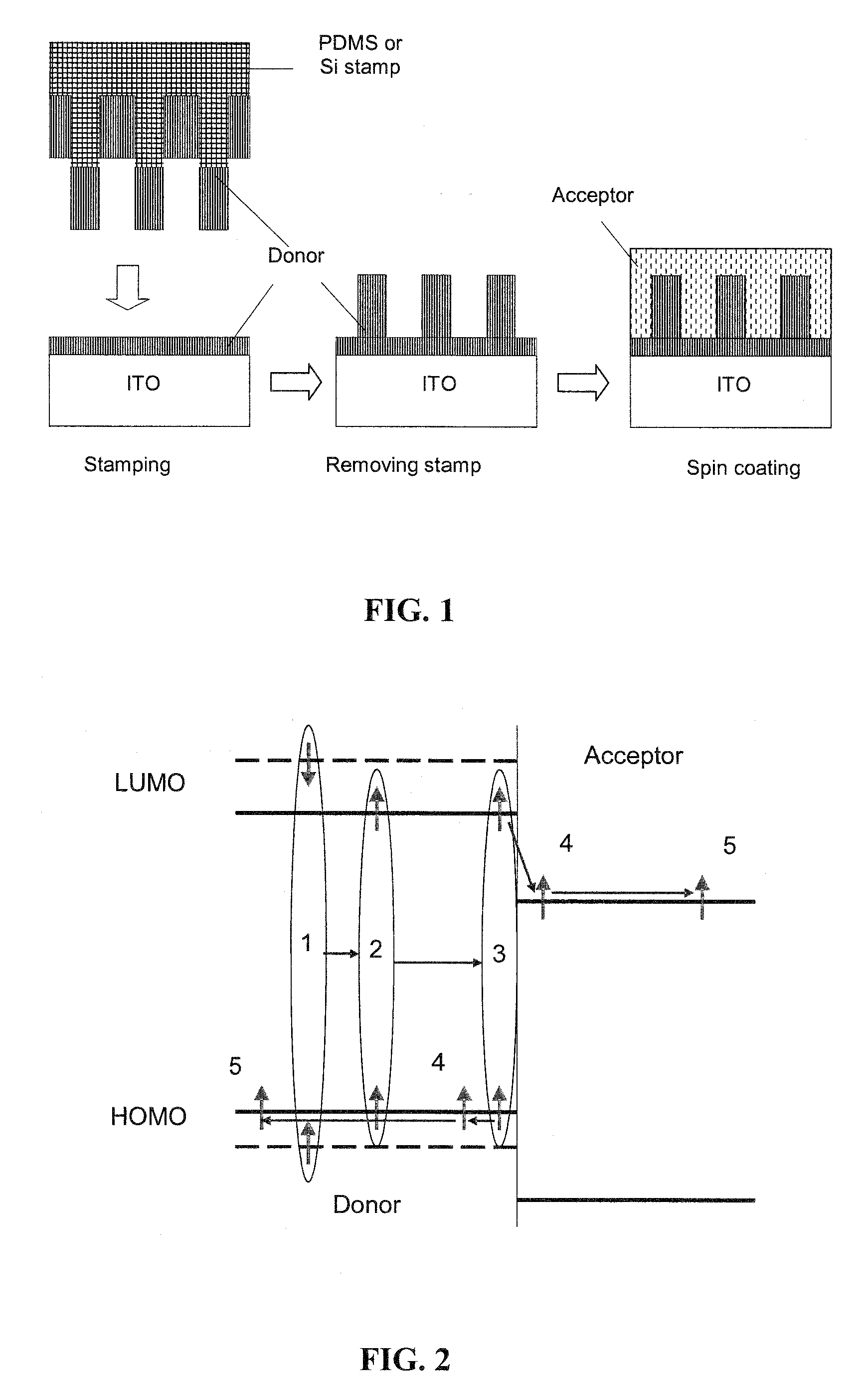
[0013]Embodiments of the invention pertain to the use of alloyed semiconductor nanocrystals for use in solar cells. The use of alloyed semiconductor nanocrystals offers materials that have a flexible stoichiometry. The alloyed semiconductor may be a ternary semiconductor alloy, such as AxB1-xC or AB1-yCy, or a quaternary semiconductor alloy, such as AxByC1-x-yD, AxB1-xCyD1-y or ABxCyD1-x-y (where A, B, C, and D are different elements). In general, alloys with more than four elements can be used as well, although it can be much harder to control the synthesis and quality of such materials. Ternary and quaternary semiconductor alloys can be formed from, but not limited to, II-VI, III-V, and I-VII compound semiconductors. Examples of such ternary alloys include, but are not limited to, ZnxCd1-xSe, CdSeyTe1-y, PbxCd1-xSe, InxGa1-xAs, and InAs1-yPy, where 02 compound semiconductors. Examples of such quaternary alloys include, but are not limited to, Cu(InxGa1-x)Se2, Cu(InxGa1-x)S2, and C...


PUM


Abstract

Embodiments of the invention pertain to the use of alloyed semiconductor nanocrystals for use in solar cells. The use of alloyed semiconductor nanocrystals offers materials that have a flexible stoichiometry. The alloyed semiconductor may be a ternary semiconductor alloy, such as AxB1-xC or AB1-yCy, or a quaternary semiconductor alloy, such as AxByC1-x-yD, AxB1-xCyD1-y or ABxCyD1-x-y (where A, B, C, and D are different elements). In general, alloys with more than four elements can be used as well, although it can be much harder to control the synthesis and quality of such materials. Embodiments of the invention pertain to solar cells having a layer incorporating two or more organic materials such that percolated paths for one or both molecular species are created. Specific embodiments of the invention pertain to a method for fabricating nanostructured bulk heterojunction that facilitates both efficient exciton diffusion and charge transport. Embodiments of the subject invention pertain to a solar cell having an architecture that allows for efficient harvesting of solar energy. The organic solar cell architecture can incorporate a host/guest (or matrix/dopant) material system that utilizes the long diffusion lengths for triplet excitons without compromising light absorption efficiency.

Description

CROSS-REFERENCE TO RELATED APPLICATION[0001]The present application claims the benefit of U.S. Provisional Application Ser. No. 60 / 939,777, filed May 23, 2007, which is hereby incorporated by reference herein in its entirety, including any figures, tables, or drawings.BACKGROUND OF INVENTION[0002]Inorganic nanocrystals have been used in hybrid organic-inorganic or all-inorganic solar cells [W. Huynh et al., Science, Vol. 295, pp. 2425-2427, 2002; I. Gur et al., Science, Vol. 310, pp. 462-465, 2005.] Power conversion efficiencies in the range of 2-3% have been demonstrated. In these devices, nanocrystals based on binary compound semiconductors are synthesized and processed in solution.[0003]To efficiently absorb light in the broad solar spectrum (spanning from ultraviolet to visible to near infrared), the energy gap of the light absorber in the solar cells needs to be optimized. At the same time, the energy level alignment between different materials in the active region will have to...

Claims


Application Information

Patent Timeline
IPC IPC(8): H01L31/0352H01L31/18H01L21/20
CPCH01L51/0004Y02E10/549H01L51/426H01L51/4213H10K71/13H10K30/10H10K30/35H10K30/20H10K30/50G03F7/0002
Inventor XUE, JIANGENG
Owner UNIV OF FLORIDA RES FOUNDATION INC
Why Eureka
Try Eureka