Photoelectric conversion device, electro-optic device, and electronic device

Active Publication Date: 2010-07-08
SEIKO EPSON CORP
View PDF1 Cites 17 Cited by
  • Summary
  • Abstract
  • Description
  • Claims
  • Application Information

AI Technical Summary

Benefits of technology

[0006]An advantage of some aspects of the invention is that it provides a photoelectric conversion device with high sensitivity and a high yield ratio. Another advant

Problems solved by technology

However, in this configuration, since the semiconductor layer (the photoelectric conversion layer) disposed directly above the contact hole is much thinner in film th

Method used


Image

  • Photoelectric conversion device, electro-optic device, and electronic device
  • Photoelectric conversion device, electro-optic device, and electronic device
  • Photoelectric conversion device, electro-optic device, and electronic device

Examples


Embodiment Construction

Photoelectric Conversion Device

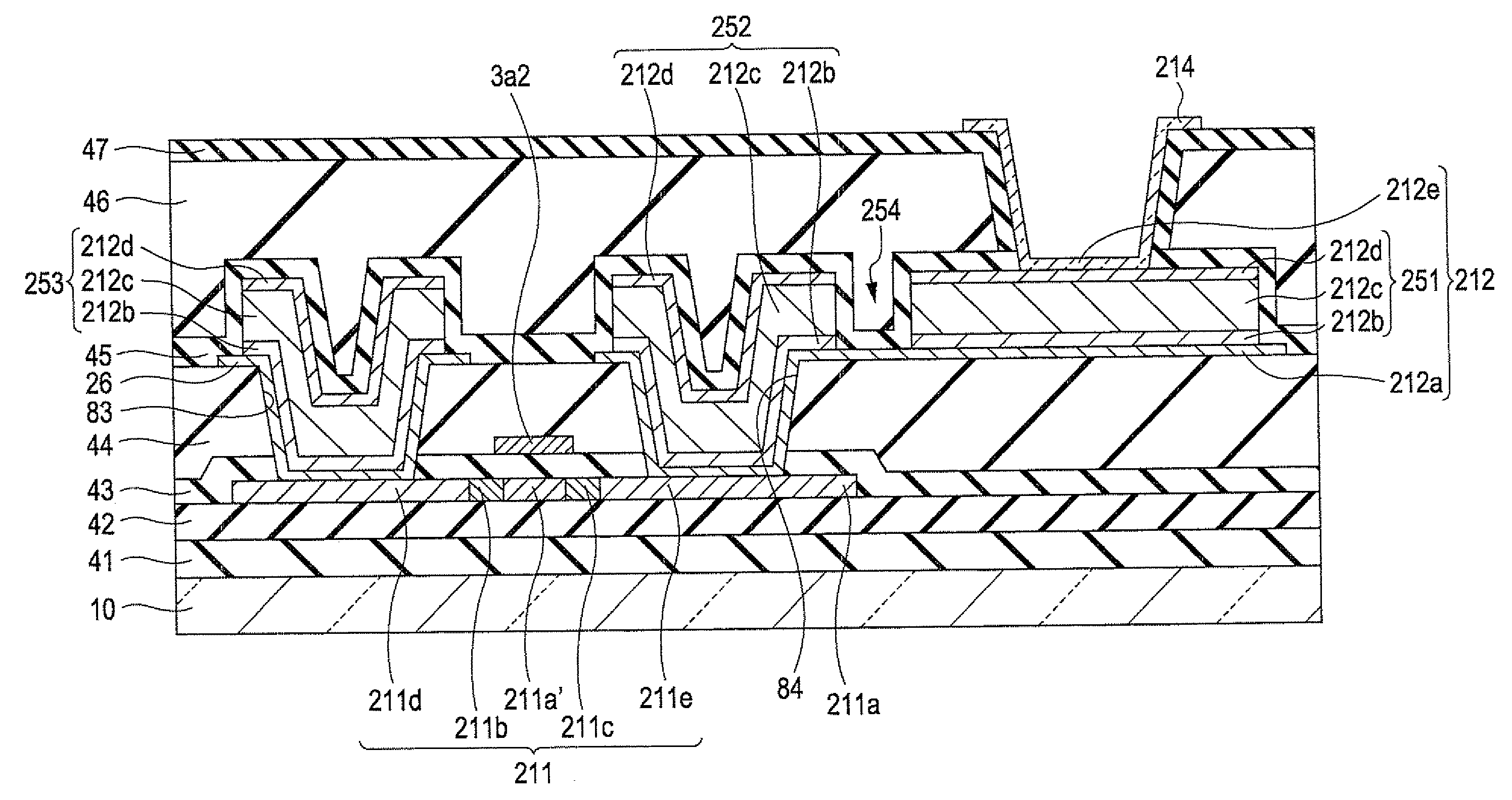
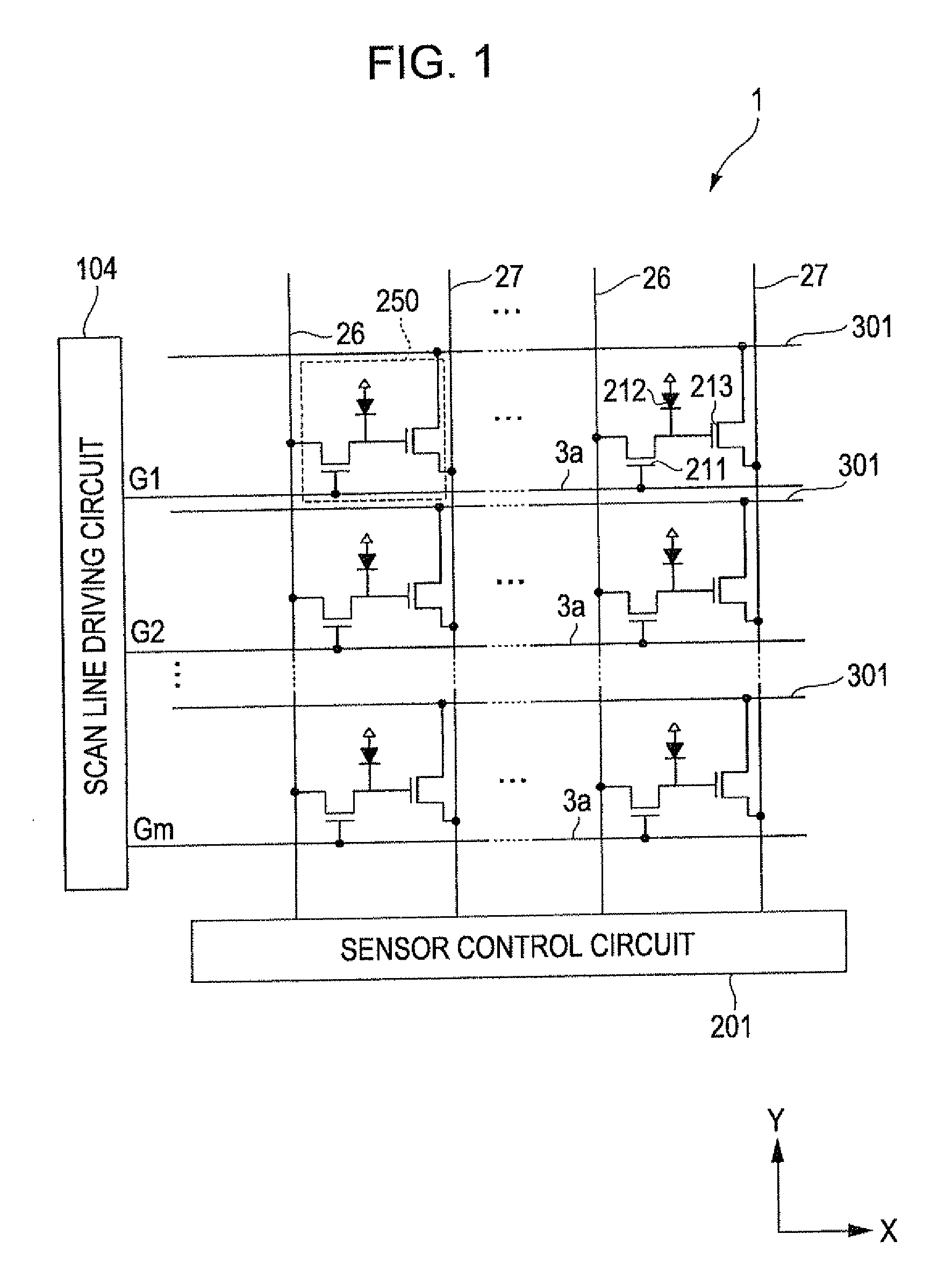
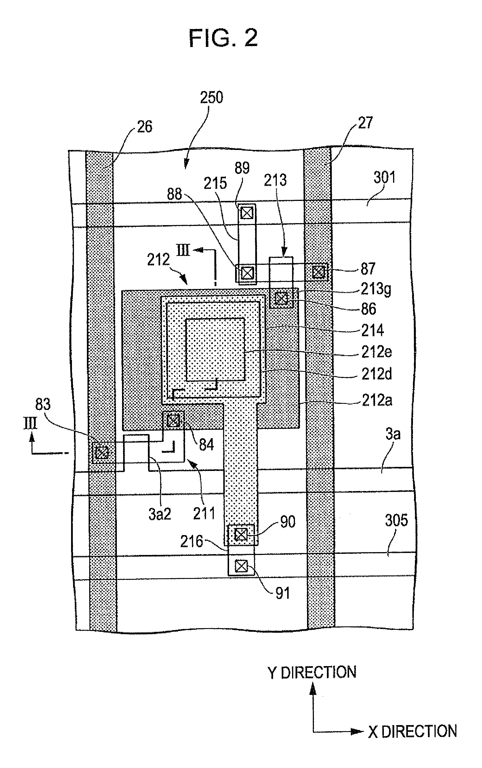
[0023]First, an image sensor 1 as an example of a photoelectric conversion device of the invention will be described with reference to FIGS. 1 to 3. FIG. 1 is an equivalent circuit of various elements and wirings of a plurality of sensors 250 which configure a light receiving area of the image sensor 1 and are formed in a matrix form. FIG. 2 is a plan view of one pixel of the image sensor 1. FIG. 3 is a cross-sectional view taken along line III-III of FIG. 2.

[0024]In FIG. 1, each of the sensors 250 formed in a matrix form includes a PIN diode 212 as an example of a “photoelectric conversion element” of the invention and TFTs 211 and 213. The sensor 250 is electrically connected to a sensor control circuit 201. The sensor control circuit 201 applies a control signal for controlling an operation of the sensor 250 to the sensor 250 via a sensor pre-charge control line 26, and an output signal including image information detected by the sensor 250 is outpu...


PUM


Abstract

The photoelectric conversion device includes: a photoelectric conversion element in which a first electrode, a photoelectric conversion layer, and a second electrode are stacked in this order; and a thin film transistor (TFT) connected to the first electrode of the photoelectric conversion element via a contact hole, wherein the photoelectric conversion layer including a first photoelectric conversion layer disposed at a location which does not overlap with the contact hole and a second photoelectric conversion layer disposed at a location which overlaps with the contact hole, the first photoelectric conversion layer and the second photoelectric conversion layer are separated from each other by a separation groove, and the second electrode is selectively formed on the first photoelectric conversion layer, and the photoelectric conversion element is formed by the first electrode, the first photoelectric conversion layer, and the second electrode.

Description

BACKGROUND[0001]1. Technical Field[0002]The present invention relates to a photoelectric conversion device, an electro-optic device, and an electronic device.[0003]2. Related Art[0004]A photoelectric conversion device is widely being used as an image sensor in facsimiles, copying machines, video cameras, and digital still cameras. Further, an electro-optic device with a built-in photoelectric conversion element in which a photoelectric conversion element is formed integrally with a pixel portion of a display panel is also been proposed (for example, see JP-A-11-121731, JP-A-2008-85029, and JP-A-2008-122659). The photoelectric conversion device and the electro-optic device commonly have a structure in which a photoelectric conversion element including a photodiode and a thin film transistor (TFT) for amplifying and extracting a signal from the photoelectric conversion element are stacked with an insulating film interposed therebetween and connected to each other via a contact hole fo...

Claims


Application Information

Patent Timeline
IPC IPC(8): H01L31/0368
CPCH01L27/14603H01L27/14634H01L27/14665
Inventor EGUCHI, TSUKASA
Owner SEIKO EPSON CORP
Why Eureka
Try Eureka