Nonvolatile magnetic memory device

a magnetic memory and non-volatile technology, applied in nanomagnetism, magnetic bodies, instruments, etc., can solve the problems of difficult microfabrication of ferroelectric layers, slow writing speed, and disadvantages of flash memory, and achieve the effects of increasing increasing the perpendicular magnetic anisotropy and the magnetic resistive of the recording layer, and easy magnetization

Inactive Publication Date: 2010-07-15
SONY CORP
View PDF13 Cites 91 Cited by
  • Summary
  • Abstract
  • Description
  • Claims
  • Application Information

AI Technical Summary

Benefits of technology

[0009]On the other hand, a perpendicular magnetization-type spin injection magnetoresistance-effect element in which the axis of easy magnetization in the recording layer is oriented in a perpendicular direction has a structure independent of shape magnetic anisotropy for retention of data, and the cell size can be reduced. However, generally, a material having crystal magnetic anisotropy in the perpendicular direction has low polarizability, and has small MR (magneto resistive). On the other hand, a material having high polarizability has crystal magnetic anisotropy in the in-plane direction, and therefore, is difficult to use for the perpendicular magnetization-type. A method for solving the problem is disclosed in JP-T-2007-525847, for example. In the method, a stress increasing layer is inserted into the recording layer provided in the spin injection magnetoresistance-effect element, and magnetic anisotropy is provided by magnetostriction. However, since the stress increasing layer is inserted into the recording layer, the magnetic characteristic is deteriorated and the polarizability is reduced, and thereby, MR may be reduced.
[0010]Therefore, there is need for a perpendicular magnetization-type nonvolatile magnetic memory device having an axis of easy magnetization in a recording layer oriented in a perpendicular direction and a configuration and a structure that can more reliably orient the axis of easy magnetization in the recording layer.
[0021]In the nonvolatile magnetic memory device according to the first embodiment of the invention, the high Young's modulus region having a Young's modulus of a higher value than that of the Young's modulus of the material forming the recording layer is provided close to the side surface of the laminated structure. Therefore, compression stress is applied to the recording layer, and the perpendicular magnetic anisotropy and the magnetic resistive of the recording layer are increased. Further, in the nonvolatile magnetic memory device according to the second embodiment of the invention, the low Young's modulus region (high stress region) having a Young's modulus of a lower value than that of the Young's modulus of the material forming the recording layer is provided above and / or below the laminated structure. Therefore, internal stress occurs in the recording layer and the perpendicular magnetic anisotropy and the magnetic resistive of the recording layer are increased. Further, as a result, the axis of easy magnetization in the recording layer can more reliably be oriented.

Problems solved by technology

However, the flash memory has a disadvantage with a slow writing speed in the order of microseconds.
The problems that the rewritable times of the FERAM are not sufficient for replacement of an SRAM or DRAM with the FERAM, and microfabrication of the ferroelectric layer is difficult are pointed out.
However, with the miniaturization of the MRAM, the bit-lines become thinner, and it is becoming difficult to flow a sufficient current.
However, with miniaturization, deterioration in data retention characteristic due to thermal disturbance becomes problematic.
Hence, in the solution, it is difficult to further reduce the cell size.

Method used


Image

  • Nonvolatile magnetic memory device
  • Nonvolatile magnetic memory device
  • Nonvolatile magnetic memory device

Examples


first embodiment

(nonvolatile magnetic memory device of the invention)

[0038]3. Example 2 (modification of example 1)

[0039]4. Example 3 (modification of example 2)

[0040]5. Example 4 (nonvolatile magnetic memory device according to second embodiment of the invention)

[0041]6. Example 5 (modification of example 4)

[0042]7. Example 6 (modification of example 4 and example 5)

[0043]8. Example 7 (another modification of example 4)

[0044]9. Example 8 (modification of example 5)

[0045]10. Example 9 (modification of example 6)

[0046]11. Example 10 (yet another modification of example 4)

[0047]12. Example 11 (still another modification of example 4 and others)

[General Explanation of Nonvolatile Magnetic Memory Device According to First Embodiment and Second Embodiment of the Invention]

[0048]A nonvolatile magnetic memory device according to the second embodiment of the invention may have a configuration in which a high Young's modulus region having a Young's modulus of a higher value than that of a Young's modulus o...

example 1

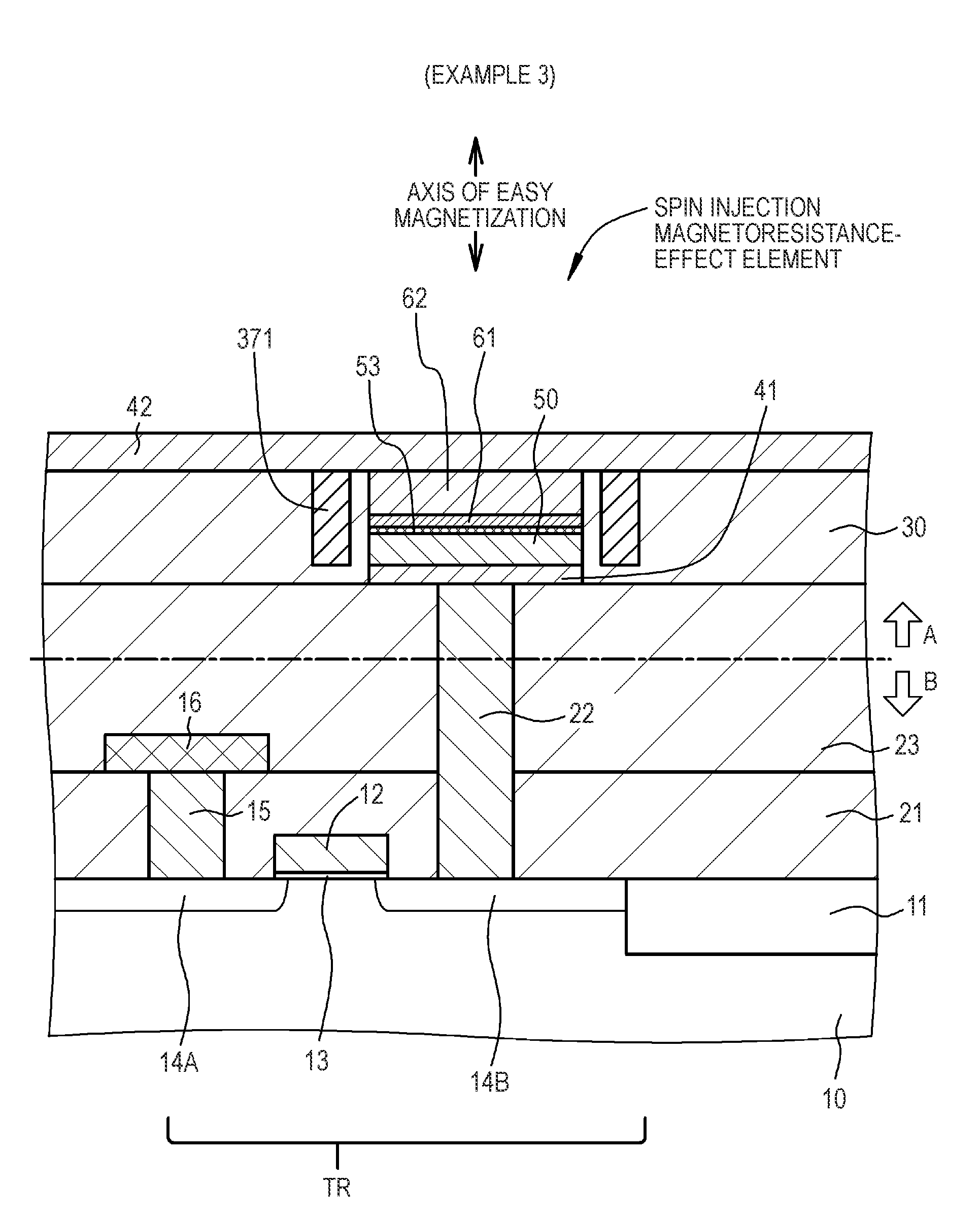
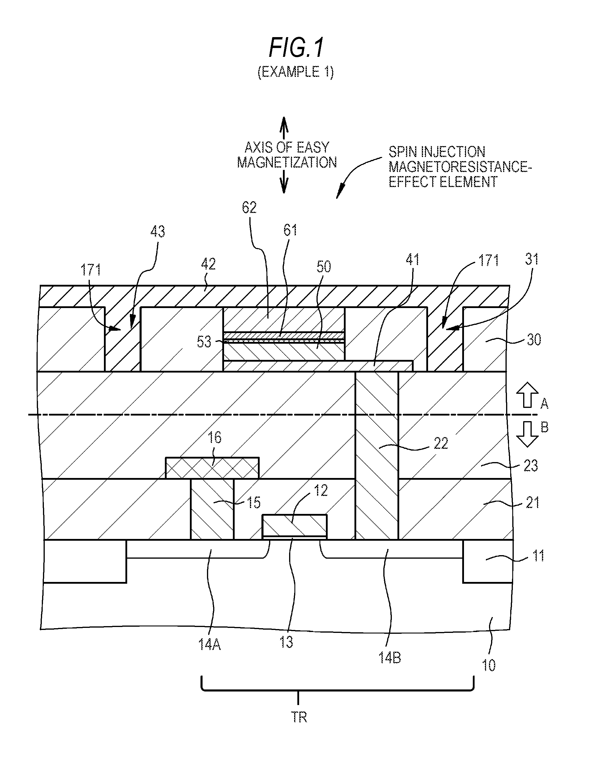
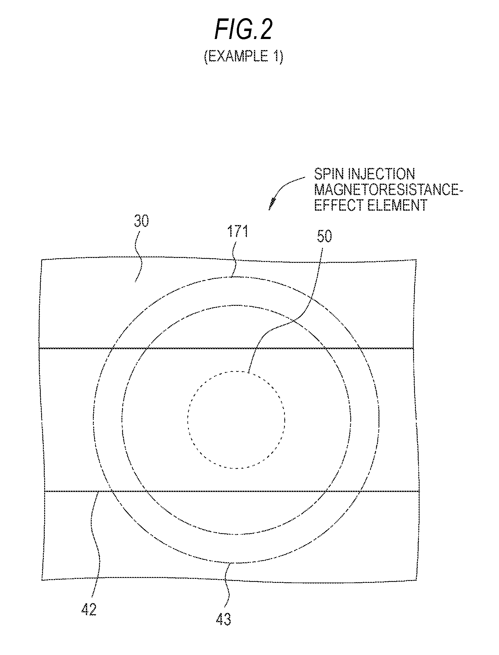
[0078]Example 1 relates to a nonvolatile magnetic memory device according to the first embodiment of the invention. FIG. 1 is a schematic partial sectional view of the nonvolatile magnetic memory device of example 1, and FIG. 2 schematically shows an arrangement condition of a laminated structure, a first wiring line, a second wiring line, and a high Young's modulus region.

[0079]The nonvolatile magnetic memory device of example 1 includes a magnetoresistance-effect element including:

[0080](A) a laminated structure 50 having a recording layer 53 in which an axis of easy magnetization is oriented in a perpendicular direction;

[0081](B) a first wiring line 41 electrically connected to a lower part of the laminated structure 50; and

[0082](C) a second wiring line 42 electrically connected to an upper part of the laminated structure 50. In example 1 to example 11, the magnetoresistance-effect element includes a spin injection magnetoresistance-effect element using magnetization reversal by...

example 2

[0128]Example 2 is a modification of example 1. FIG. 3 is a schematic partial sectional view of a nonvolatile magnetic memory device of example 2. In example 2, a high Young's modulus region 271 having a Young's modulus of a higher value than that of the Young's modulus of the material forming the recording layer 53 is also provided close to the side surface of the laminated structure 50. However, unlike in example 1, in example 2, an insulator film 32 is formed on the side surface of the laminated structure 50, and the high Young's modulus region 271 is formed to have a sidewall shape via the insulator film 32 on the side surface of the laminated structure 50.

[0129]In example 2, the high Young's modulus region 271 includes tungsten nitride (WN). On the other hand, the second wiring line 42 includes titanium (Ti). Values of the Young's modulus EH of the high Young's modulus region 271 etc. are shown in table 2.

[0130]Regarding the nonvolatile magnetic memory device of example 2, subs...


PUM


Abstract

A nonvolatile magnetic memory device having a magnetoresistance-effect element includes: (A) a laminated structure having a recording layer in which an axis of easy magnetization is oriented in a perpendicular direction; (B) a first wiring line electrically connected to a lower part of the laminated structure; and (C) a second wiring line electrically connected to an upper part of the laminated structure, wherein a high Young's modulus region having a Young's modulus of a higher value than that of a Young's modulus of a material forming the recording layer is provided close to a side surface of the laminated structure.

Description

BACKGROUND OF THE INVENTION[0001]1. Field of the Invention[0002]The present invention relates to a nonvolatile magnetic memory device.[0003]2. Description of Related Art[0004]With the remarkable proliferation of information and communication equipment, particularly, personal small items such as portable terminals, various kinds of semiconductor devices of memory elements and logic elements forming the equipment are requested to have higher performance of higher integration, higher speed, lower power consumption, and the like. Especially, a nonvolatile memory is considered to be indispensable for the ubiquitous age. Even in exhaustion or trouble of a power supply, or disconnection between a server and a network due to some failure, important information can be saved and protected by the nonvolatile memory. Further, the recent portable equipment is designed to suppress the power consumption as much as possible by allowing an unnecessary circuit block to stand by. If a nonvolatile memo...

Claims


Application Information

Patent Timeline
Patent Type & Authority Applications(United States)
IPC IPC(8): H01L29/82
CPCB82Y25/00G11C11/16H01F10/3286H01F10/3263H01L43/02H01F10/3254G11C11/161H10B61/22H10N50/80H10N50/10H10N50/85
Inventor SHOJI, MITSUHARU
Owner SONY CORP
Why Eureka
Try Eureka