Gallium oxide film and heteroepitaxial growth method and application thereof

A technology of heteroepitaxy and growth methods, applied in the field of semiconductor epitaxy, can solve the problems of lack of symmetry, small size, heteroepitaxial lattice mismatch, etc., to solve the problem of small nucleation size, avoid dislocations and cracks, reduce The effect of lattice mismatch

Pending Publication Date: 2021-03-12
SUZHOU INST OF NANO TECH & NANO BIONICS CHINESE ACEDEMY OF SCI
View PDF0 Cites 2 Cited by
  • Summary
  • Abstract
  • Description
  • Claims
  • Application Information

AI Technical Summary

Problems solved by technology

[0008] From the above technical solutions, it can be seen that the gallium oxide crystal thin film epitaxy on the gallium oxide homogeneous substrate can avoid problems such as lattice mismatch, and the quality of the thin film crystal is high, but the preparation of the gallium oxide homogeneous substrate is difficult, and the It is even more difficult to grow, and the price is expensive, so it is difficult to carry out practical promotion and application
[0009] Although heteroepitaxy can overcome the shortcomings of small size and high cost, generally speaking, the direct lattice mismatch and thermal expansion coefficient mismatch of different materials will lead to film cracking, high defect density, and poor crystal quality; currently, heteroepitaxial gallium oxide Film quality is still far from practical application
For example, compared to hexagonal systems such as sapphire and gallium nitride, monoclinic β-Ga 2 o 3 Lack of symmetry, there is a "sixfold domain" problem caused by "in-plane twist" during heteroepitaxial growth, which makes it difficult to improve the crystal quality of heteroepitaxial thin films
[0010] Overall, the current Ga 2 o 3 The heteroepitaxy of thin film materials is still immature and cannot meet the requirements of device applications; and there are problems such as lattice mismatch in heteroepitaxy, which requires technological breakthroughs to achieve high-quality Ga 2 o 3 Epitaxial Growth and Application of Crystal Thin Film

Method used


Image

  • Gallium oxide film and heteroepitaxial growth method and application thereof
  • Gallium oxide film and heteroepitaxial growth method and application thereof
  • Gallium oxide film and heteroepitaxial growth method and application thereof

Examples


Embodiment 1

[0066] Embodiment 1 gallium oxide heteroepitaxy (random growth) on sapphire substrate

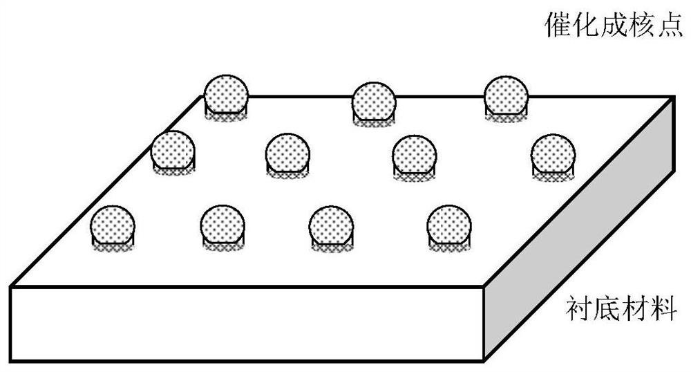
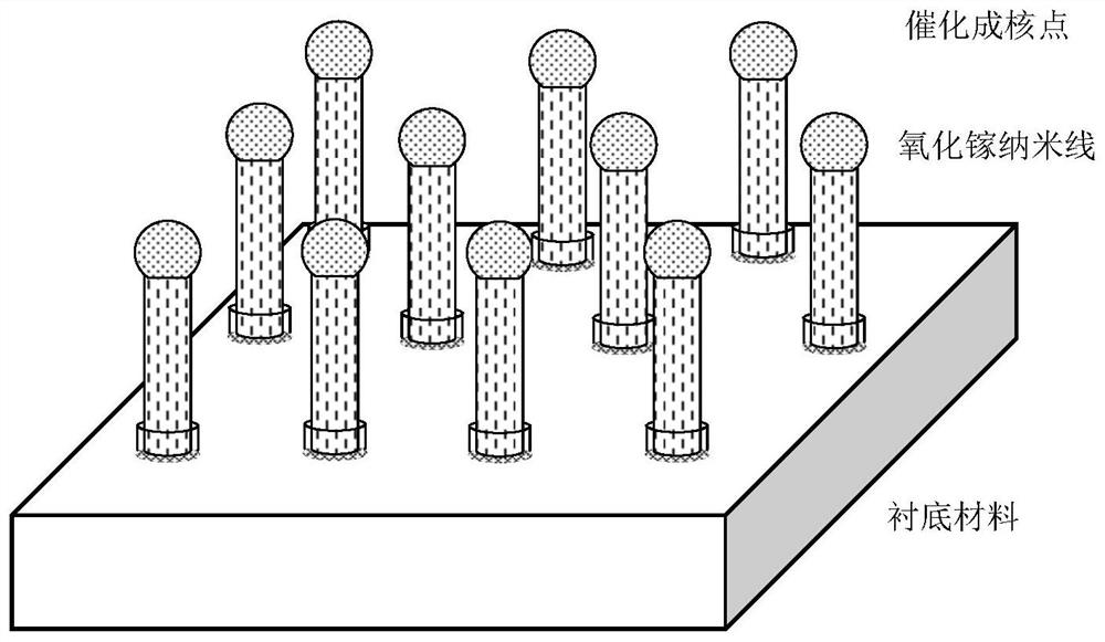
[0067] (1) if figure 1 As shown, at 300-1000 °C, the nano-metal catalytic particles dispersed on the substrate dissolve with the gaseous source of the growth material to form eutectic alloy droplets; then the alloy droplets dissolve the component atoms of the growth material, and when the alloy droplets After the component atoms in the supersaturation, crystallization begins at the boundary between the droplet and the substrate, and promotes the movement of the catalytic droplet, thereby growing one-dimensional nanowire materials (such as figure 2 shown).

[0068] (2) During the growth of nanowires, nanoscale low-melting catalytic droplets are formed. These catalytic droplets are generally eutectic alloys formed by metal particles and reactant materials. Commonly used metal catalysts include Au, Ag, Ni, Pt, etc. . If the element of the catalytic droplet is a certain element of the growt...

Embodiment 2

[0070] Example 2 Gallium oxide heteroepitaxy (patterned growth) on sapphire substrate

[0071] (1) Preparation of deposition dielectric mask layer and catalyst positioning

[0072] Deposit a layer of silicon oxide dielectric (gallium nitride, aluminum oxide, etc.) mask with a film thickness of 1-1000nm, and use photolithography, etching, or focused ion beam to open holes in the dielectric mask; or use an already patterned A thin substrate material is used as a growth template for gallium oxide nanowires, such as a porous anodic aluminum oxide film (AAO, Anodic Aluminum Oxide Template).

[0073] (2) Gallium oxide nanowire epitaxy

[0074] Send the patterned substrate material into the MOCVD reaction chamber for the growth of gallium oxide nanowires, and deposit Ga droplets as catalysts; use the catalytic effect of Ga droplets to epitaxy Ga 2 o 3 array of nanowires. Growth equipment is not limited to material growth equipment such as MOCVD, LPCVD, and PVD.
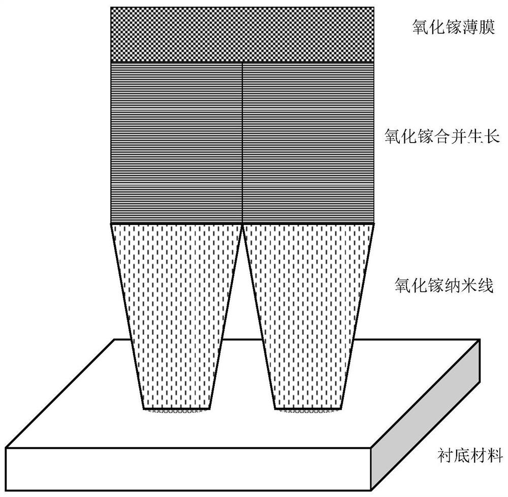
[0075] (3) Merg...


PUM

PropertyMeasurementUnit
diameteraaaaaaaaaa
heightaaaaaaaaaa
thicknessaaaaaaaaaa

Abstract

The invention discloses a gallium oxide film and a heteroepitaxial growth method and application thereof. The heteroepitaxial growth method comprises the following steps: carrying out vapor phase epitaxial growth on a substrate material to form a gallium oxide nanowire array; and, by controlling the growth conditions, enabling the gallium oxide nanowires in the gallium oxide nanowire array to transversely merge and grow, thereby forming the gallium oxide thin film on the gallium oxide nanowire array through epitaxial growth. According to the invention, the gallium oxide nanowire arrays are combined to grow the beta Ga2O3 film, so that the [beta]-Ga2O3 film is prevented from directly growing on the substrate, the mismatch degree between heteroepitaxial materials and the difficulty of a heteroepitaxial process are greatly reduced, and the crystal quality of the [beta]-Ga2O3 film is improved; and by controlling the diameter and the period of the gallium oxide nanowire, the grain nucleation size can be well increased, the influence of the small nucleation size on the crystal quality is avoided, the growth of the [beta]-Ga2O3 film can be realized at the temperature of 300 DEG C-1000 DEGC, and the energy consumption can be effectively reduced.

Description

technical field [0001] The present invention relates to the technical field of semiconductor epitaxy, in particular to the technical field of controllable epitaxy preparation of nanomaterials, in particular to a gallium oxide thin film and its heterogeneous epitaxy growth method and application. Background technique [0002] Semiconductor materials play an irreplaceable role in the modern information industrialized society and are the cornerstone of the modern semiconductor industry and microelectronics industry. With the continuous development of various advanced technologies, the demand for high-performance electronic devices such as high withstand voltage, high power, and radiation resistance, as well as deep ultraviolet optoelectronic devices is becoming more and more urgent, especially in the fields of high withstand voltage and deep ultraviolet. Materials have been difficult to meet the requirements of use. [0003] The third-generation semiconductor materials, such a...

Claims


Application Information

Patent Timeline
Patent Type & Authority Applications(China)
IPC IPC(8): H01L21/02H01L29/24
CPCH01L21/0242H01L21/02483H01L21/02513H01L21/02565H01L29/24
Inventor 张晓东马永健李军帅张宝顺
Owner SUZHOU INST OF NANO TECH & NANO BIONICS CHINESE ACEDEMY OF SCI
Why Eureka
Try Eureka