Image display device

a display device and image technology, applied in semiconductor devices, instruments, computing, etc., to achieve the effect of reducing crosstalk or ghosting

Inactive Publication Date: 2010-07-22
KYOCERA CORP
View PDF12 Cites 31 Cited by
  • Summary
  • Abstract
  • Description
  • Claims
  • Application Information

AI Technical Summary

Benefits of technology

[0004]The present invention aims to provide an image display device that can reduce crosstalk or ghost caused by a parasitic capacitance between an image signal line and a storage capacitance.Means For Solving Problem

Problems solved by technology

When there is a parasitic capacitance between the image signal line and the capacitive element, the potential retained by the capacitive element varies due to the parasitic capacitance during a threshold-voltage detecting period for detecting the threshold voltage of each pixel or during a light-emitting period in which an organic EL element of each pixel emits light, whereby a problem arises such as the generation of crosstalk or ghost.

Method used


Image

  • Image display device
  • Image display device
  • Image display device

Examples


Embodiment Construction

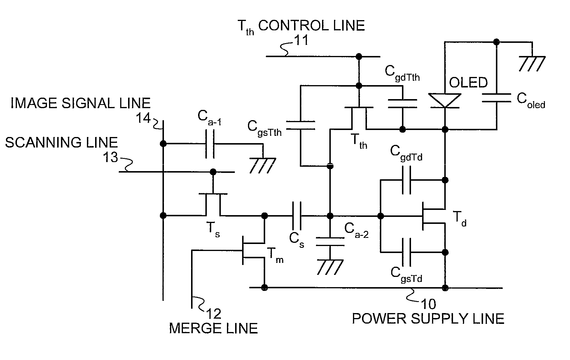
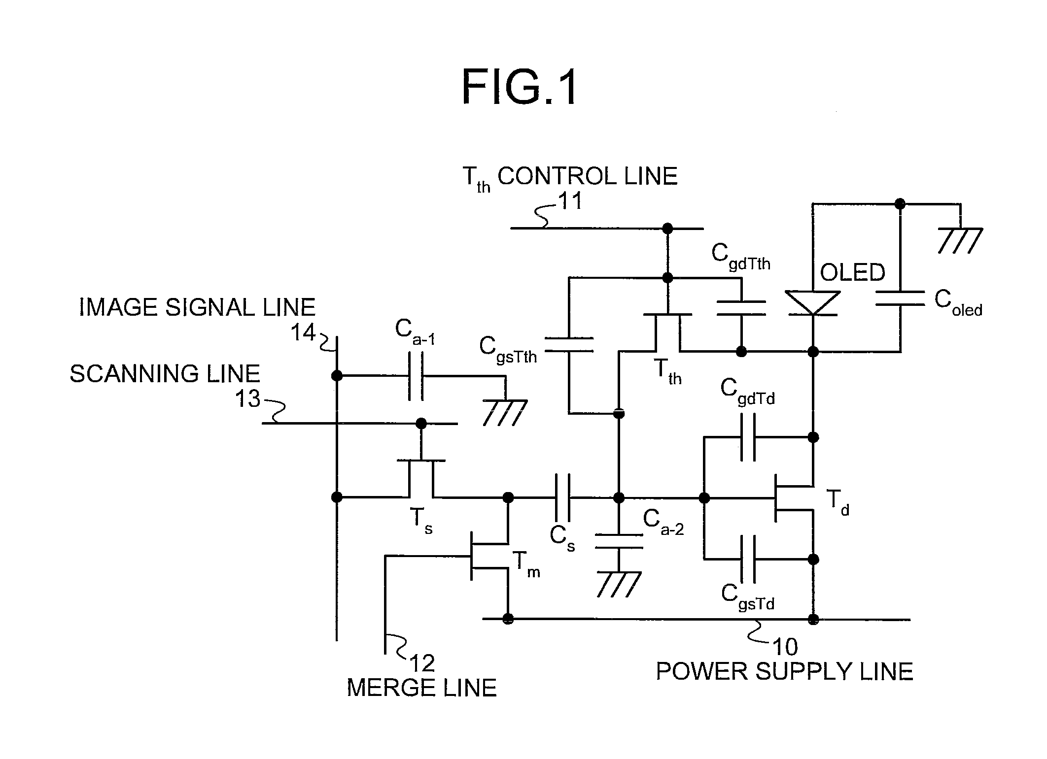
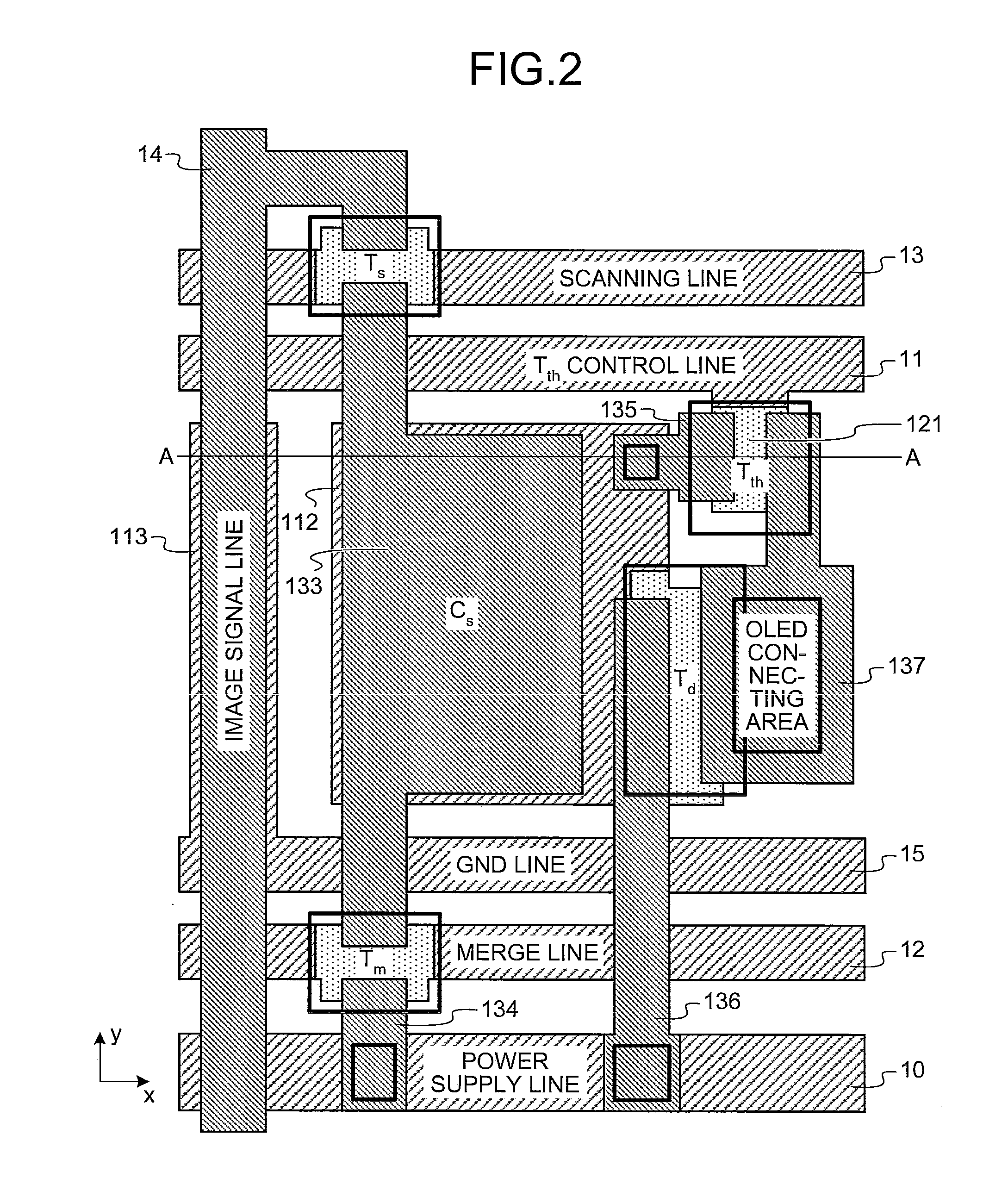
[0024]FIG. 8-1 is a circuit diagram for explaining a pixel circuit corresponding to one pixel in an image display device according to one embodiment of the present invention. FIG. 8-2 is a diagram in which parasitic capacitances are written in the pixel circuit illustrated in FIG. 8-1. The pixel circuit illustrated in FIG. 8-1 includes an organic EL element OLED, a drive transistor Td, a threshold-voltage detecting transistor Tth, a storage capacitance Cs, a switching transistor Ts, and a switching transistor Tm.

[0025]The drive transistor Td is a control element for controlling an amount of current flowing through the organic EL element OLED according to the potential difference applied between a gate electrode and a source electrode. The threshold-voltage detecting transistor Tth has a function of electrically connecting a gate electrode to a drain electrode of the drive transistor Td, when the transistor Tth is turned on. The transistor Td also has a function of detecting a thresh...


PUM


Abstract

According to one embodiment, an image display device includes: a plurality of pixels including a light-emitting element, a driver element that controls light emission of the light-emitting element, and a capacitive element electrically connected to the driver element; and an image signal line that is commonly connected to the pixels for sequentially supplying, to the pixels, an image signal corresponding to luminous brightness of the light-emitting element. The pixel includes a shield electrode that shields an electric field from the image signal line to the capacitive element.

Description

TECHNICAL FIELD[0001]The present invention relates to an image display device such as an organic electroluminescence (EL) display device.BACKGROUND ART[0002]There has conventionally been proposed an image display device employing a current control type organic EL element that has a function of generating light due to the recombination of a hole and an electron injected into a luminescent layer. As the image display device of this type, there has conventionally been known the one in which a pixel circuit including four thin film transistors (hereinafter referred to as TFT) made of amorphous silicon, polycrystalline silicon and so on, and an organic EL element formed of an organic light emitting diode and so on, forms one pixel (see, for example, Japanese Patent Application Laid-open No. 2006-209074). In the image display device disclosed in Japanese Patent Application Laid-open No. 2006-209074, a threshold voltage of a drive transistor which drives an organic EL element is detected, ...

Claims


Application Information

Patent Timeline
Patent Type & Authority Applications(United States)
IPC IPC(8): G09G3/30G06F3/038
CPCG09G3/3233G09G2300/0819G09G2300/0842G09G2300/0866G09G2320/0209G09G2320/0223G09G2320/043H01L27/3272H01L27/124H10K59/126H01L27/1214G09G2300/0861
Inventor TAKASUGI, SHINJIEBISUNO, KOHEI
Owner KYOCERA CORP
Why Eureka
Try Eureka