

Plasma processing apparatus
a technology of processing apparatus and plasma, which is applied in the direction of coating, chemical vapor deposition coating, electric discharge tube, etc., to achieve the effect of increasing the amount of radical generation and preventing particle generation
- Summary
- Abstract
- Description
- Claims
- Application Information
AI Technical Summary
Benefits of technology
Problems solved by technology
Method used
Image

Examples
first embodiment
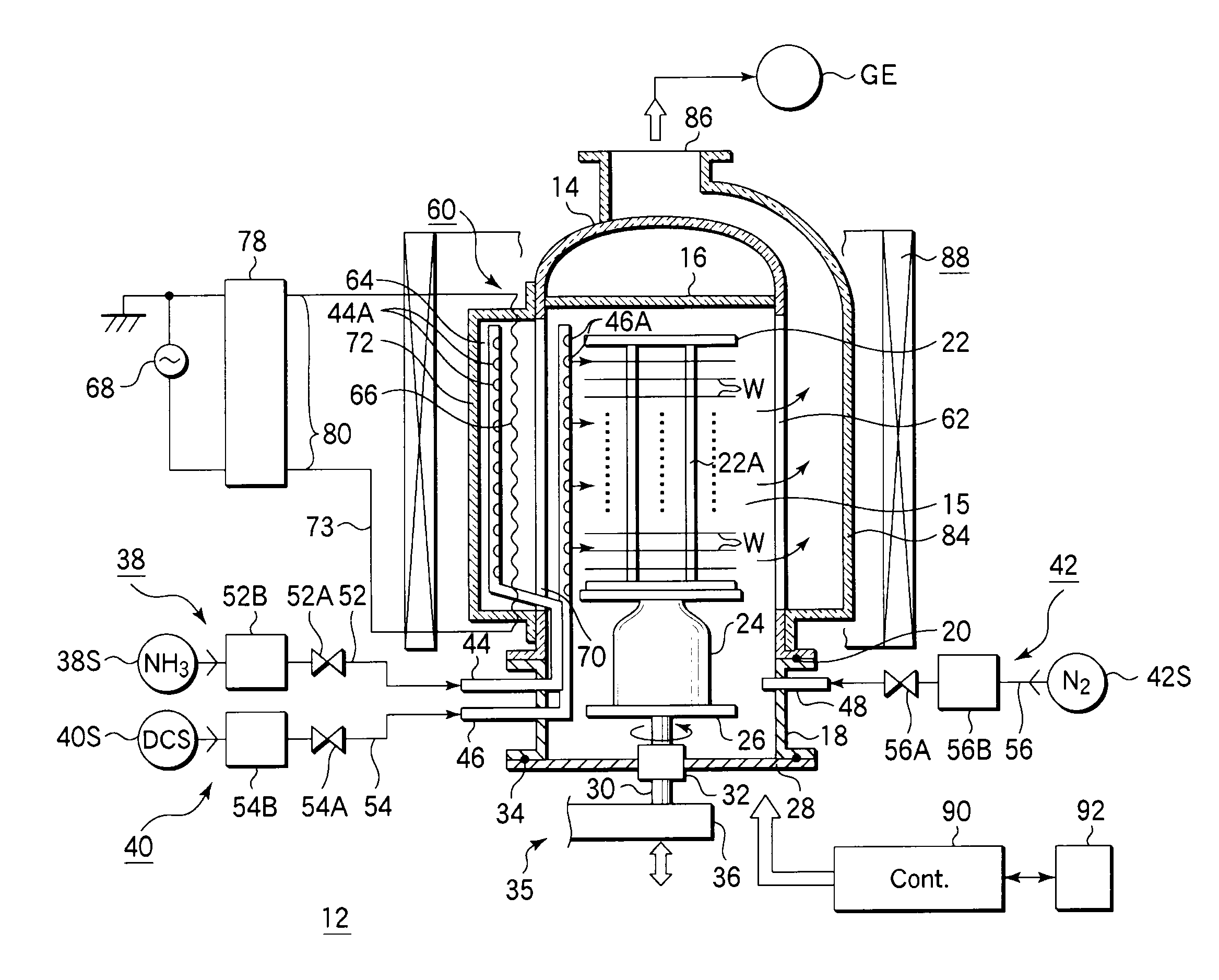
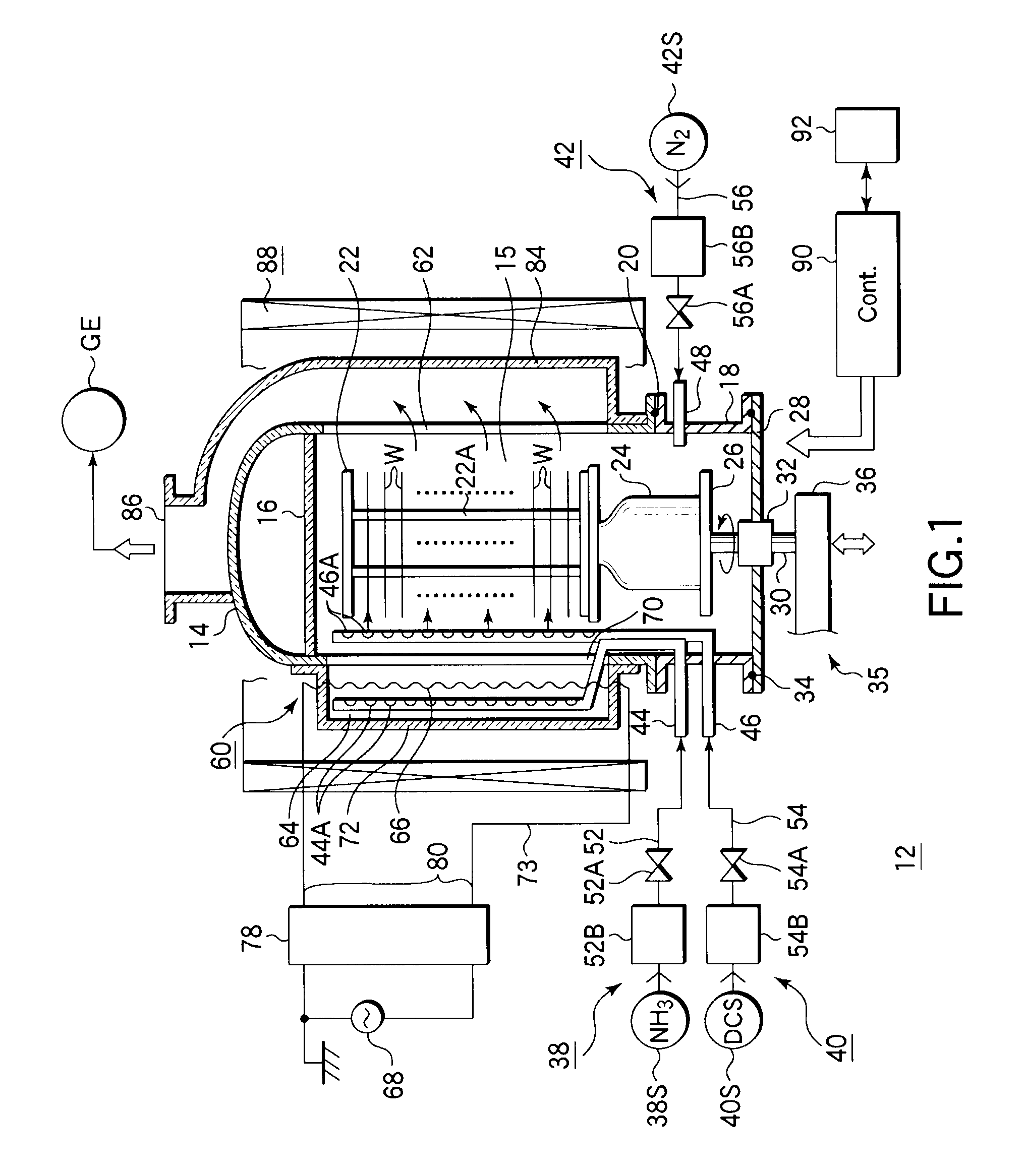
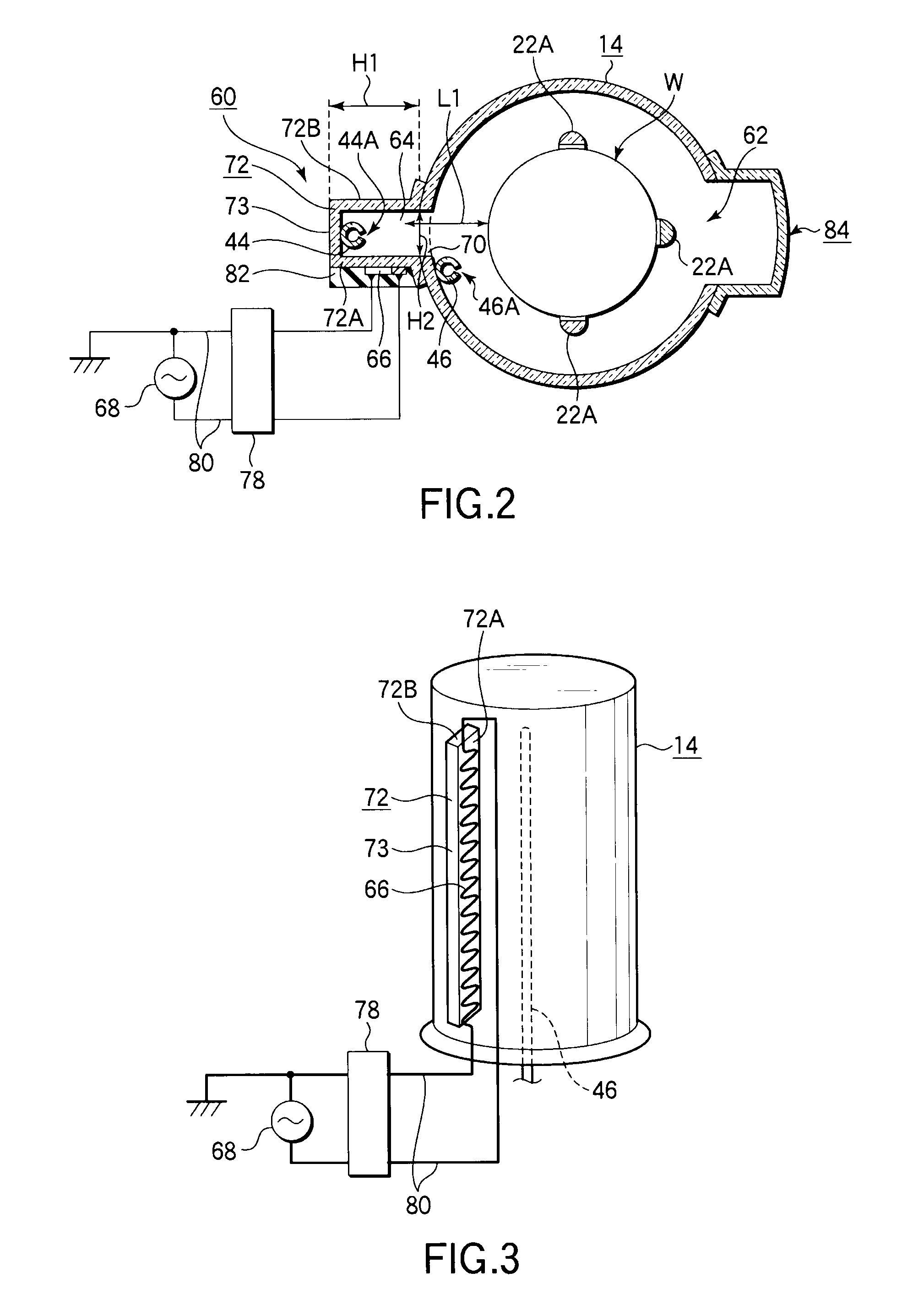
[0045]FIG. 1 is a sectional front view showing a vertical plasma processing apparatus according to a first embodiment of the present invention. FIG. 2 is a sectional plan view showing part of the apparatus shown in FIG. 1 (excluding the heater). FIG. 3 is a schematic perspective view showing the process container of the apparatus shown in FIG. 1 provided with an ICP electrode. FIGS. 4A and 4B are enlarged views showing part of the ICP electrode of the apparatus shown in FIG. 1. The film formation apparatus 12 has a process field configured to be selectively supplied with a first process gas containing dichlorosilane (DCS) gas as a silane family gas, and a second process gas containing ammonia (NH3) gas as a nitriding gas. The film formation apparatus 12 is configured to form a silicon nitride film on target objects in the process field, while activating the NH3 gas by use of plasma.
[0046]The apparatus 12 includes a process container 14 shaped as a cylindrical column with a ceiling a...
second to sixth embodiment
[0087]FIGS. 6A to 6E are enlarged plan views each showing a meandering electrode used in a plasma processing apparatus, according to second to sixth embodiments of the present invention, respectively. In the first embodiment, the meandering electrode 66 has the bent portions 74 each having an arc shape. Alternatively, meandering electrodes 66 shown in FIGS. 6A to 6E may be used.
[0088]In the second embodiment shown in FIG. 6A, the electrode 66 comprises bent portions 74 each having an elliptic arc shape, and the bent portions 74 are connected to each other to alternately face opposite directions to form a meandering shape as a whole. The meandering shape of the electrode 66 is not limited to a specific one, and it may be formed by use of, e.g., a cycloid curve or sine curve.
[0089]In the third embodiment shown in FIG. 6B, the meandering electrode 66 is formed of bent portions 74 and straight line portions 100 each having a predetermined length. The bent portions 74 and straight line p...
seventh embodiment
[0094]FIG. 7 is a schematic perspective view showing a main portion of a plasma processing apparatus according to a seventh embodiment of the present invention. In the first to sixth embodiments described above, the electrode 66 is disposed outside one of the sidewalls 72A and 72B. On the other hand, in the seventh embodiment shown in FIG. 7, the electrode 66 is disposed outside the backside wall 73.
[0095]All the other portions of this embodiment may be designed as described in the first embodiment. The electrode 66 of this embodiment may be one of those described with reference to the first to sixth embodiments. This embodiment can also exhibit the same function and effect as the first embodiment.
PUM
| Property | Measurement | Unit |
|---|---|---|
| distance | aaaaa | aaaaa |
| diameter | aaaaa | aaaaa |
| thickness | aaaaa | aaaaa |
Abstract
Description
Claims
Application Information