Method of manufacturing silicon substrate

a manufacturing method and silicon technology, applied in the direction of crystal growth process, after-treatment details, water-setting substance layered product, etc., can solve the problems of significant deterioration of device characteristics, difficult to perform sufficient precipitation in a substrate, and the rear surface of a substrate is likely to be scratched, so as to prevent the occurrence of white spots, improve the yield of a solid-state imaging device, and prevent the effect of white spots

Inactive Publication Date: 2009-09-10
SUMCO CORP
View PDF11 Cites 8 Cited by
  • Summary
  • Abstract
  • Description
  • Claims
  • Application Information

AI Technical Summary

Benefits of technology

[0017]When the silicon substrate is used to manufacture a solid-state imaging device, it is possible to prevent the occurrence of defects in a transistor and a buried photodiode of the solid-state imaging device due to heavy metal contamination, and it is possible to prevent the generation of white spots in the solid-state imaging device. As a result, it is possible to improve the yield of a solid-state imaging device.
[0018]Therefore, according to the present invention, since the silicon substrate has high gettering capability, it is possible to provide a silicon substrate capable of reducing the influence of metal contamination. Therefore, it is possible to reduce manufacturing costs and prevent the generation of particles in a device process.

Problems solved by technology

When impurities, such as heavy metal, are mixed with the silicon substrate, device characteristics significantly deteriorate.
In this case, it is difficult to perform sufficient precipitation in a substrate to obtain gettering capability.
However, when pre-annealing is performed before an epitaxial process, scratches are likely to occur in the rear surface of a substrate.
As a result, the function of gettering sinks is likely to deteriorate.

Method used


Image

  • Method of manufacturing silicon substrate
  • Method of manufacturing silicon substrate
  • Method of manufacturing silicon substrate

Examples


Embodiment Construction

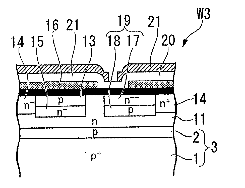
[0028]Hereinafter, a silicon substrate and a method of manufacturing the same according to an embodiment of the present invention will be described with reference to the accompanying drawings.

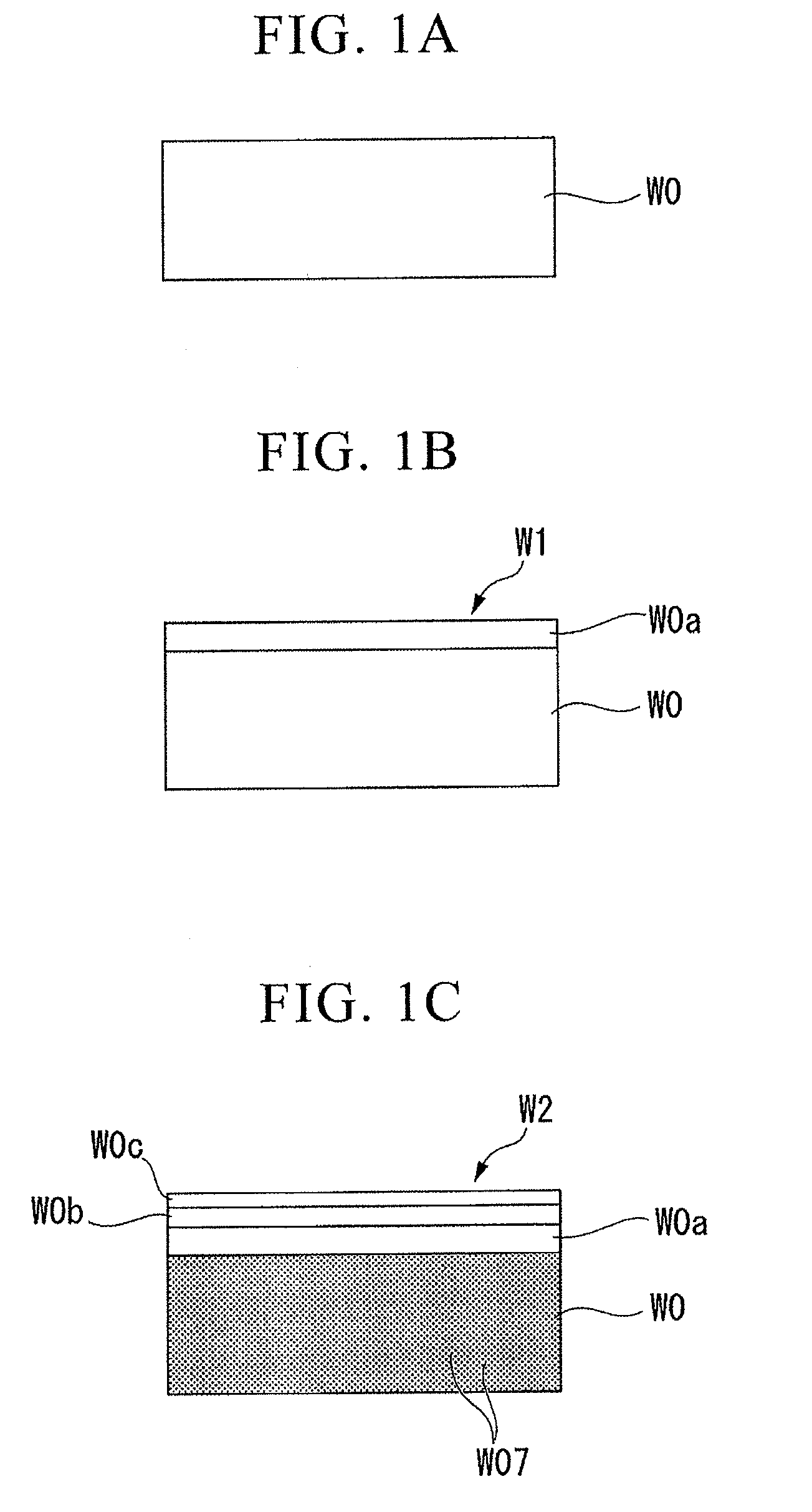
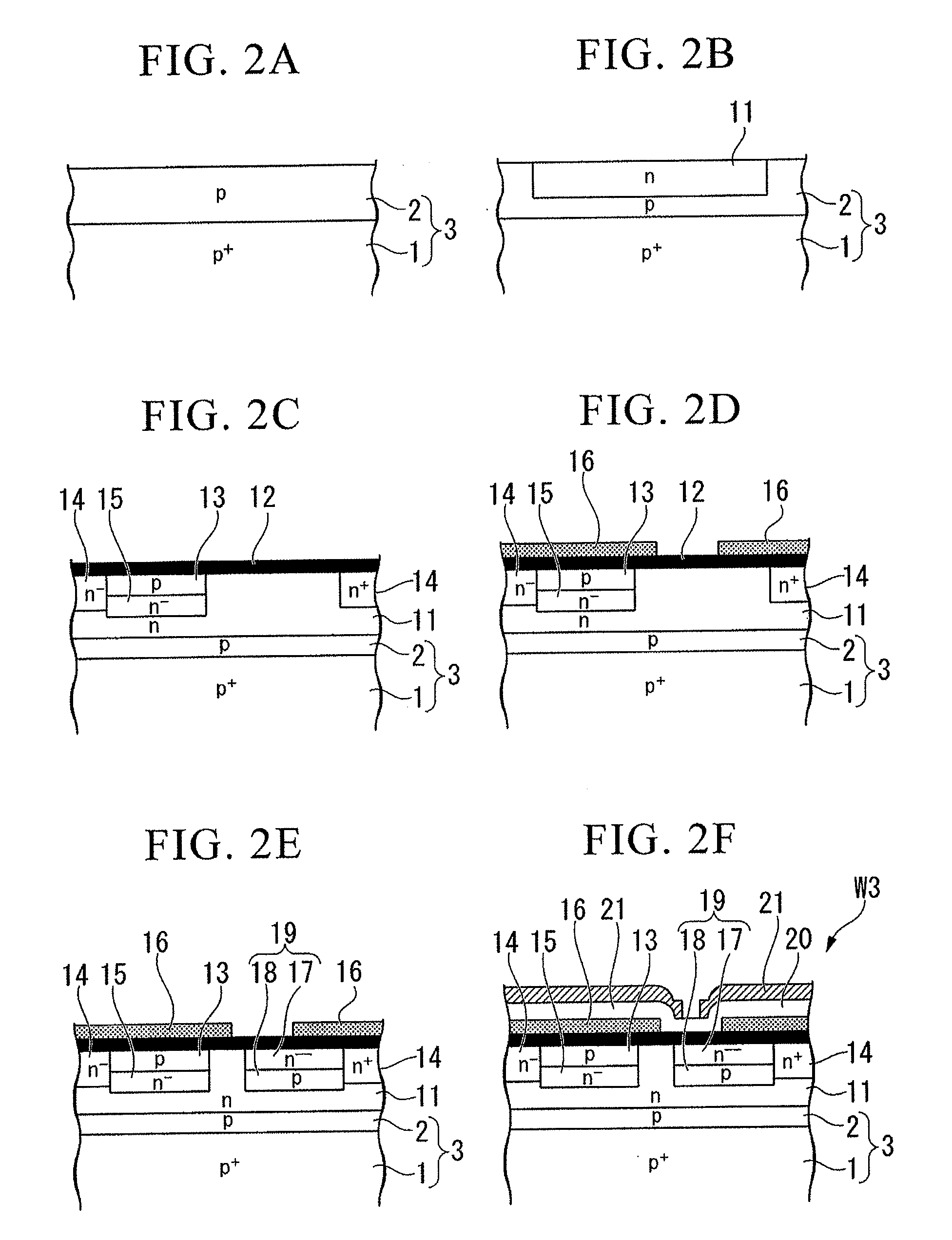
[0029]FIGS. 1A to 1C and FIGS. 2A to 2F are front cross-sectional views illustrating processes of a method of manufacturing a silicon substrate according to this embodiment, and FIG. 3 is a flowchart illustrating the method of manufacturing a silicon substrate according to this embodiment. In the drawings, reference numeral W0 denotes a silicon substrate.

[0030]In this embodiment, a silicon substrate used to manufacture a solid-state imaging device will be described.

[0031]As shown in FIG. 3, the manufacturing method according to this embodiment includes a wafer manufacturing process including a silicon single crystal pulling step S1, a wafer processing step S2, an epitaxial layer forming step S3, and a post-annealing step S4, and a device step S5.

[0032]In the example shown in FIGS. 1A to 1C, fir...


PUM

PropertyMeasurementUnit
temperatureaaaaaaaaaa
sizeaaaaaaaaaa
thicknessaaaaaaaaaa

Abstract

A method of manufacturing a silicon substrate includes: growing a silicon single crystal having a carbon concentration in the range of 1.0×10¹⁶ atoms/cm3 to 1.6×10¹⁷ atoms/cm3 and an initial oxygen concentration in the range of 1.4×10¹⁸ atoms/cm3 to 1.6×10¹⁸ atoms/cm3 using a CZ method; slicing the silicon single crystal; forming an epitaxial layer on the sliced silicon single crystal; and performing a heat treatment thereon as a post-annealing process at a temperature in the range of 600° C. to 850° C.

Description

BACKGROUND OF THE INVENTION[0001]1. Field of the Invention[0002]The present invention relates to a method of manufacturing a silicon substrate, and more particularly, to a technique applicable for a silicon substrate that has a high gettering capability and is used to manufacture a device, such as a solid-state imaging device.[0003]Priority is claimed on Japanese Patent Application No. 2008-054843, filed Mar. 5, 2008, the content of which is incorporated herein by reference.[0004]2. Description of Related Art[0005]A thin semiconductor device made of silicon is manufactured by slicing a silicon single crystal pulled by, for example, a CZ (Czochalski) method into a silicon substrate and forming a circuit on the silicon substrate. When impurities, such as heavy metal, are mixed with the silicon substrate, device characteristics significantly deteriorate.[0006]For example, impurities, such as heavy metal, are mixed with the silicon substrate by the following causes: first, metal contami...

Claims


Application Information

Patent Timeline
Patent Type & Authority Applications(United States)
IPC IPC(8): B32B13/04H01L21/205
CPCC30B15/00C30B33/02C30B29/06C30B15/04H01L21/208
Inventor KURITA, KAZUNARIOMOTE, SHUICHI
Owner SUMCO CORP
Why Eureka
Try Eureka