Low threading dislocation density relaxed mismatched epilayers without high temperature growth

a dislocation density and low threading technology, applied in the direction of single crystal growth, polycrystalline material growth, chemistry apparatus and processes, etc., can solve the problems of difficult depositing high germanium concentration alloys without deleterious, problematic material combinations in processing, etc., to avoid the generation of germane particles and low threading

Inactive Publication Date: 2005-03-08
TAIWAN SEMICON MFG CO LTD
View PDF223 Cites 8 Cited by
  • Summary
  • Abstract
  • Description
  • Claims
  • Application Information

AI Technical Summary

Benefits of technology

The problems of the prior art can be overcome by developing a method to create high dislocation velocities even though deposition occurs at lower growth temperatures. Accordingly, the invention provides

Problems solved by technology

However, just as the different materials properties are beneficial from the system application perspective, other properties may make such materials combinations problematic in processing.
Therefore, upon deposition of one semiconductor material on top of another substrate material can result in many defects in the semiconductor layer, rendering it useless for practical application.
However, practical constraints from current equipment used to manufacture Si-based epitaxial layers create difficulty in depositing high germanium concentration alloys without deleterious particle formation from either gas phase nucleation or equipment coating.
Although these systems offer great control of Si

Method used


Image

  • Low threading dislocation density relaxed mismatched epilayers without high temperature growth
  • Low threading dislocation density relaxed mismatched epilayers without high temperature growth
  • Low threading dislocation density relaxed mismatched epilayers without high temperature growth

Examples


Embodiment Construction

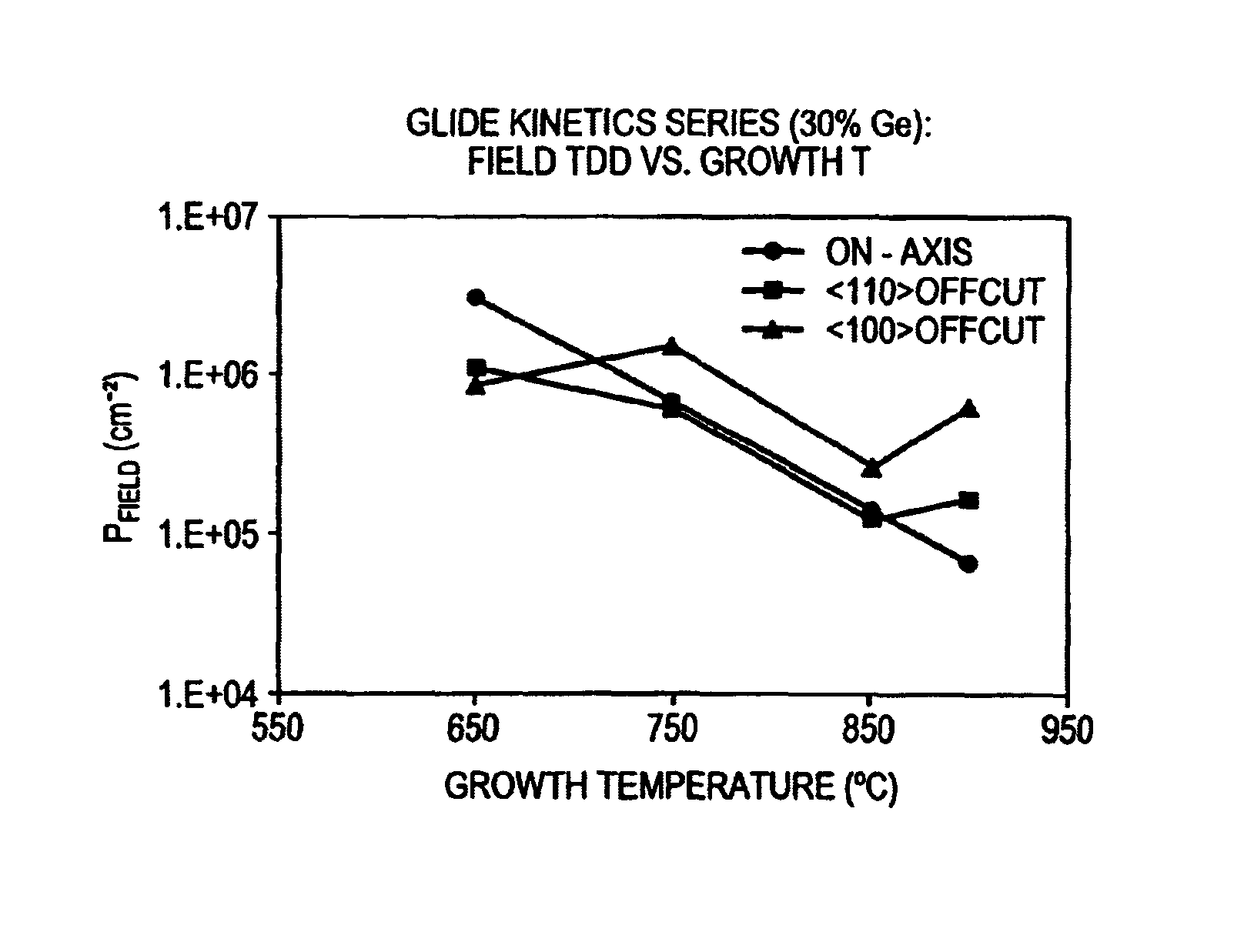
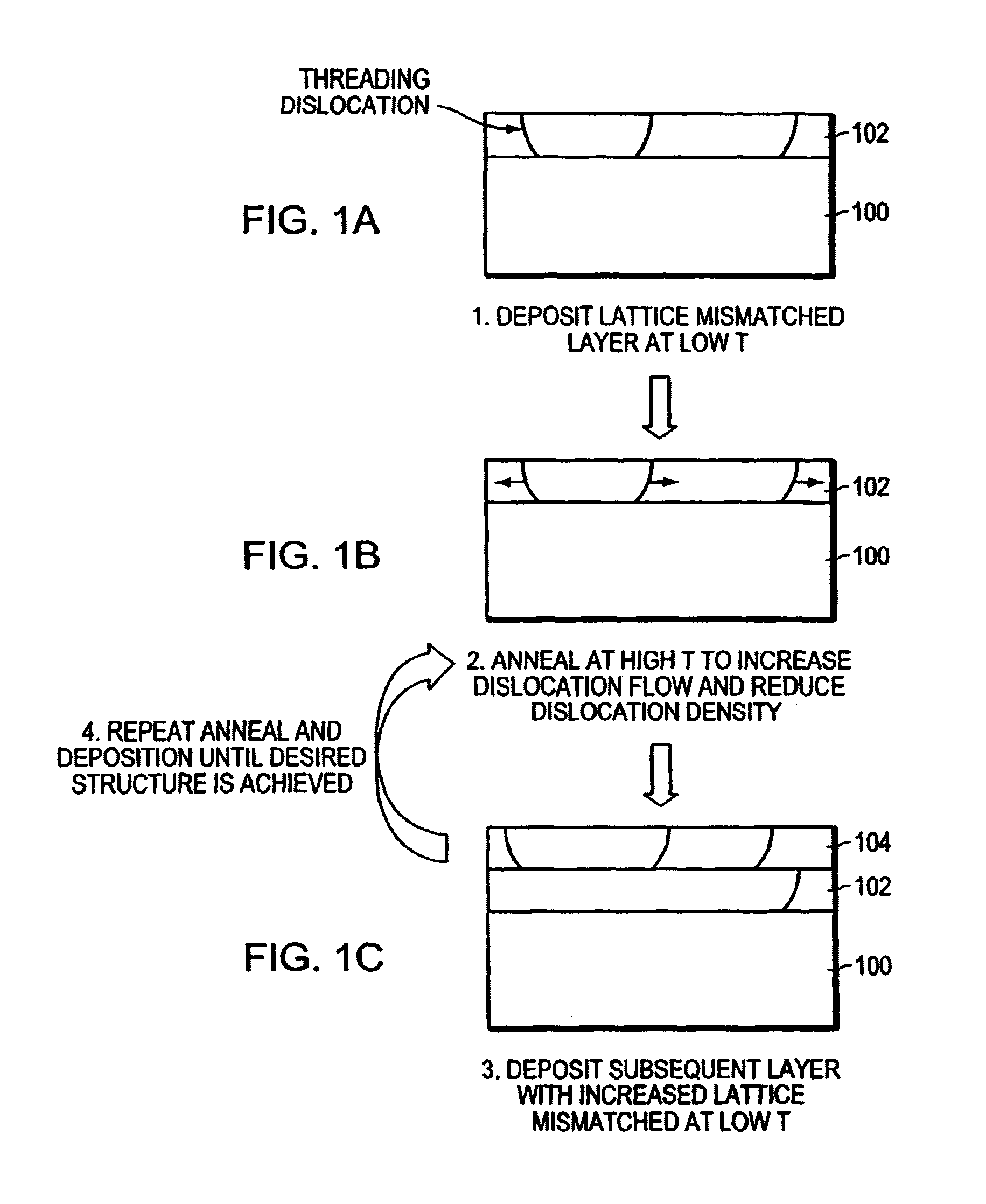
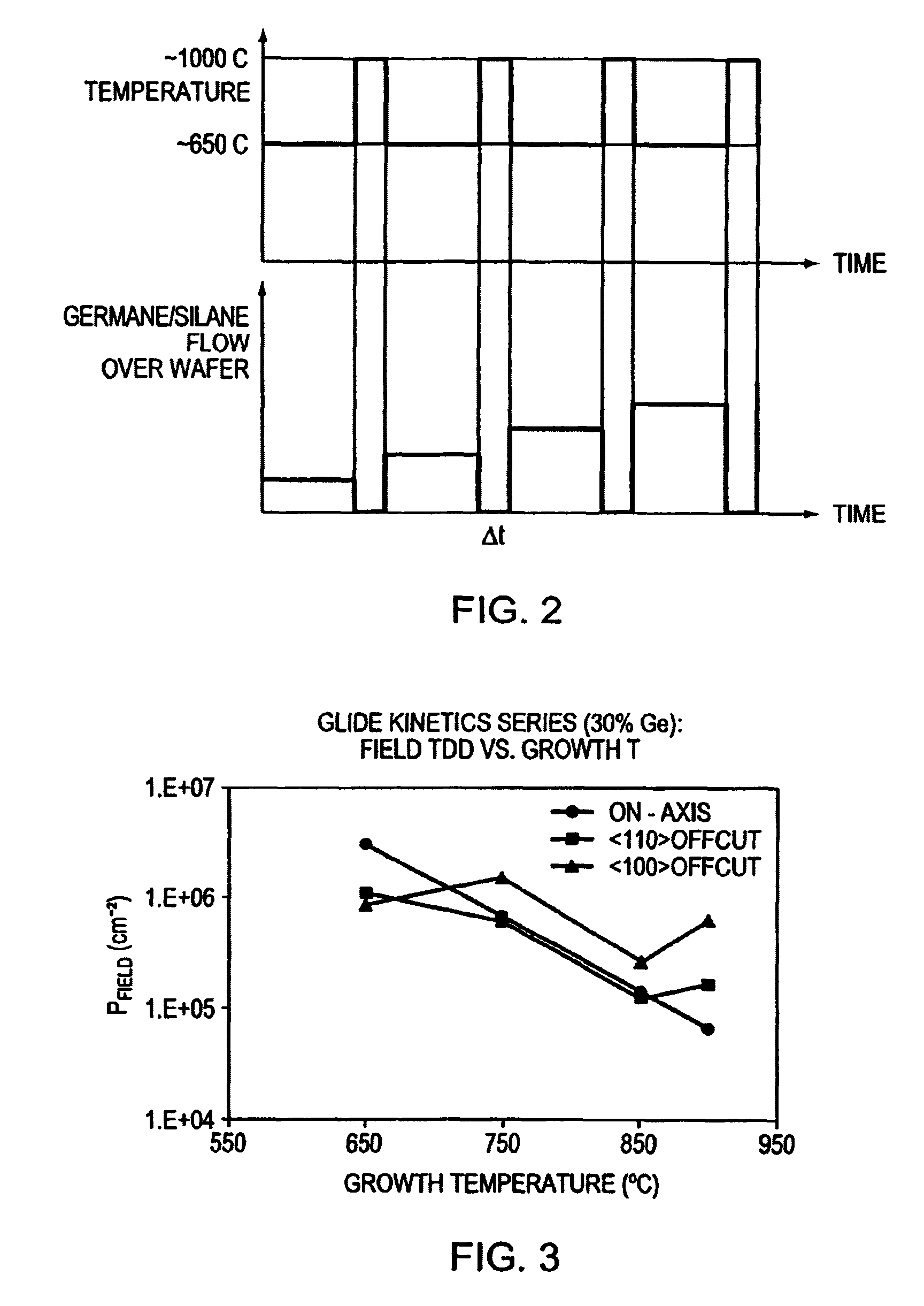
FIGS. 1A-1C is a schematic block diagram of the growth process and subsequent structure of low dislocation density, lattice mismatched films using alternating steps of epitaxial growth and high temperature annealing. In accordance with an exemplary embodiment of the invention, a relatively low lattice-mismatched film 102 is deposited on a surface of a substrate 100 with a different lattice constant at a low temperature, i.e., where particle generation is at a minimum. A low mismatched film can be defined as one in which the lattice mismatch is less than 1%.

After deposition of the film 102, the film is annealed at high temperature without any deposition source gas flowing across the surface, i.e., hydrogen or nitrogen, since they do not deposit any atoms on the surface. This annealing step increases dislocation flow and nearly completely relaxes the deposited film. Because the mismatch is low, the threading dislocation density remains low. Also, the rapid thermal feature of many CVD ...


PUM


Abstract

A semiconductor structure and method of processing same including a substrate, a lattice-mismatched first layer deposited on the substrate and annealed at a temperature greater than 100° C. above the deposition temperature, and a second layer deposited on the first layer with a greater lattice mismatch to the substrate than the first semiconductor layer. In another embodiment there is provided a semiconductor graded composition layer structure on a semiconductor substrate and a method of processing same including a semiconductor substrate, a first semiconductor layer having a series of lattice-mismatched semiconductor layers deposited on the substrate and annealed at a temperature greater than 100° C. above the deposition temperature, a second semiconductor layer deposited on the first semiconductor layer with a greater lattice mismatch to the substrate than the first semiconductor layer, and annealed at a temperature greater than 100° C. above the deposition temperature of the second semiconductor layer.

Description

BACKGROUND OF THE INVENTIONThe invention relates to the field of low threading dislocation density relaxed mismatched epilayers, and in particular to such epilayers grown without high temperature.The goal of combining different materials on a common substrate is desirable for a variety of integrated systems. Specifically, it has been a long-standing desire to combine different semiconductor and oxide materials on a common useful substrate such as a silicon substrate. However, just as the different materials properties are beneficial from the system application perspective, other properties may make such materials combinations problematic in processing. For example, semiconductor materials with different properties often have different lattice constants. Therefore, upon deposition of one semiconductor material on top of another substrate material can result in many defects in the semiconductor layer, rendering it useless for practical application.Seminal work into the quantitative in...

Claims


Application Information

Patent Timeline
IPC IPC(8): C30B25/02H01L21/20H01L21/02H01L21/205
CPCC30B25/02H01L21/0262C30B29/42C30B29/52H01L21/02381H01L21/02392H01L21/02395H01L21/0245H01L21/02461H01L21/02463H01L21/02505H01L21/0251H01L21/02532H01L21/02543H01L21/02546C30B29/40
Inventor FITZGERALD, EUGENE A.
Owner TAIWAN SEMICON MFG CO LTD
Why Eureka
Try Eureka