Fluorescent material,scintillator using same, and radiation detector using same

a fluorescence material and scintillator technology, applied in the direction of fluorescence/phosphorescence, conversion screens, optical radiation measurement, etc., can solve the problems of reducing the use efficiency of x-rays, vibration from the exterior vibrating the electrode plate, and high internal pressure of the xenon gas filled chamber, so as to reduce the afterglow level and reduce the scan time. , the effect of increasing resolution

Active Publication Date: 2010-07-29
HITACHI METALS LTD
View PDF3 Cites 21 Cited by
  • Summary
  • Abstract
  • Description
  • Claims
  • Application Information

AI Technical Summary

Benefits of technology

[0085]A fluorescent material according to the present invention is able to provide a scintillator having a low level of afterglow 1 to 10 ms after the termination of X-ray radiation, as compared with a conventional fluorescent material of GGAG:Ce. A radiation detector according to the present invention, formed using such a fluorescent material as a scintillator, has a shorter scan time. The detector may contribute thereby to increased resolution. The detector may also have stable detection performance.BEST MODE FOR CARRYING OUT THE PRESENT INVENTION
[0086]The inventor studied in detail the causes of the above problem. It was thereby found that when a fluorescent material of GGAG:Ce was excited by a predetermined light, thereby producing an afterglow spectrum, the long wavelength component of 750 to 850 nm therein was correlated with the short term afterglow of the fluorescent material. This enabled the inventor to achieve the present invention.
[0087]The afterglow from X-ray excitation is proportional to the afterglow from ultraviolet ray excitation. In view of this, a study was conducted to find out why the level of afterglow increases by use of a fluorescence spectrophotometer (F4500 manufactured by Hitachi Co. Ltd.).
[0088]FIG. 1 is directed to the case in which a GGAG:Ce single crystal grown using a CZ method is excited using an ultraviolet light at a wavelength of 260 nm as an excitation light. FIG. 1 is a schematic diagram of a fluorescent spectrum in this case. The GGAG:Ce single crystal contains an ion Ce3+. This ion Ce3+ exhibits a smoothly curved fluorescent spectrum. The spectrum peaks at a wavelength of 540 nm. The fluorescence around a wavelength of 315 nm and the fluorescence around a wavelength of 400 nm are thought to be due to defects in the lattice. On the other hand, a weak, broad fluorescence is observed in the range of wavelengths of 700 to 850 nm.
[0089]FIG. 2 is a schematic diagram of afterglow profiles for each wavelength in this fluorescent material. That is, FIG. 2 shows change in the fluorescence intensity after stopping emitting excitation light. As can be seen from the figure, the fluorescence at the wavelength of 315 nm causes a very low level of afterglow. Similarly, the fluorescence at the wavelengths of 400 nm causes a very low level of afterglow. However, the fluorescence at the wavelength of 800 nm causes a very high level of afterglow.
[0090]FIG. 3 is directed to the case in which a sample of a GGAG:Ce polycrystal sintered by using an HIP sintering method is excited using an ultraviolet light at a wavelength of 260 nm as a excitation light. FIG. 3 is a schematic diagram of a fluorescent spectrum in this case. The GGAG:Ce material contains an ion Ce3+. This ion Ce3+ exhibits a smoothly curved fluorescent spectrum. The spectrum peaks at a wavelength of 540 nm. The fluorescence around a wavelength of 380 nm is thought to result from an overlap of the fluorescence due to defects in the lattice and the fluorescence caused by Ce3+ incorporated in a perovskite phase constituting a heterogeneous phase in the GGAG:Ce polycrystal. When a perovskite phase is detected using an X-ray diffraction method, the fluorescence at this wavelength of 380 nm appears strongly. However, even when a perovskite phase is not detected at all, this fluorescence appears. On the other hand, a weak, broad fluorescence is observed in the range of wavelengths of 700 to 850 nm.

Problems solved by technology

However, the interior pressure of the xenon gas filled chamber is high.
This decreases use efficiency of X-rays.
However, if the electrode plate is thin, vibration from the exterior vibrates the electrode plate.
This generates noise.
This constitutes a problem.
This causes noise in a silicon photodiode.
This in turn decreases the sensitivity.
However, an increase in the thickness thereof hinders miniaturization of an X-ray detecting element.
This increases the cost.
All this causes an X-ray detecting element to have a shortened integration time.

Method used


Image

  • Fluorescent material,scintillator using same, and radiation detector using same
  • Fluorescent material,scintillator using same, and radiation detector using same
  • Fluorescent material,scintillator using same, and radiation detector using same

Examples


first embodiment

[0100]A fluorescent material according to the first embodiment of the present invention comprises Ce as an activator and further comprises at least Gd, Al, Ga, O, Fe, and a component M, wherein the component M is at least one of Mg, Ti, Ni. The composition of the fluorescent material is expressed by the general formula:

(Gd1-x-zLuxCez)3+a(Al1-u-sGauScs)5−aO12

wherein

[0101]0≦a≦0.15,

[0102]0≦x≦0.5,

[0103]0.0003≦z≦0.0167,

[0104]0.2≦u≦0.6, and

[0105]0≦s≦0.1,

and wherein, regarding the concentrations of Fe and the component M,

[0106]0.05≦Fe concentration (mass ppm)≦1, and

[0107]0≦M concentration (mass ppm)≦50.

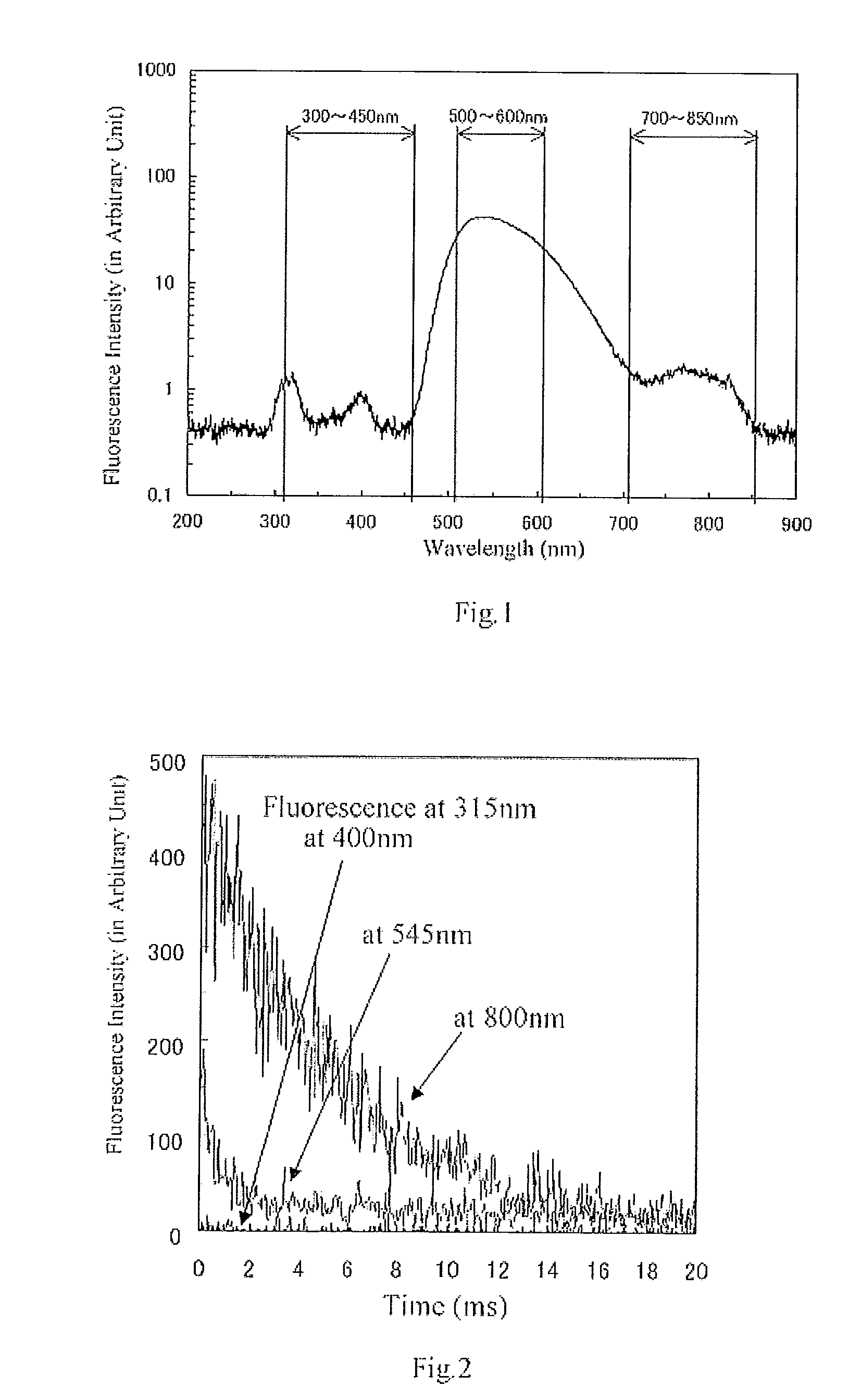
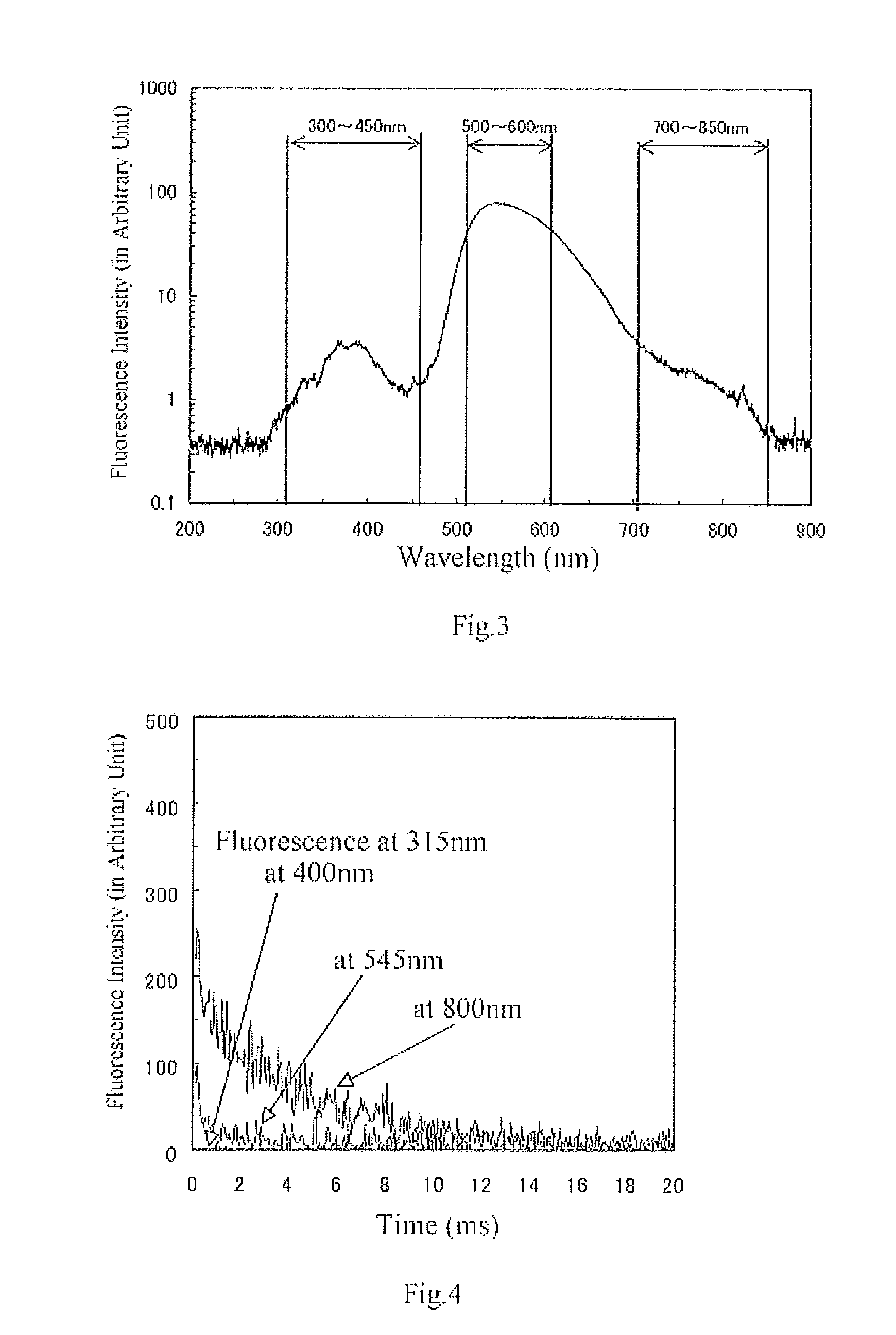
[0108]This material according to the present invention must contain Fe. The content of Si ranges from 0.05 to 1 mass ppm. FIG. 7 shows that when the content of Fe exceeds 1 mass ppm, this causes the 3 ms afterglow to exceed 800 ppm. Therefore, the after glow exceeds the tolerance level. This causes the upper limit of the content of Fe to be set at 1 mass ppm. However, the upper limit is pre...

second embodiment

[0143]A fluorescent material according to the second embodiment of the present invention contains Ce as a fluorescent activator. In addition, the material contains at least Gd, Al, Ga, and O. In addition, the material contains Lu and / or Y. The composition of the material is expressed by the following general formula.

(Gd1-x-zLxCez)3+a(Al1-uGau)5−aO12

wherein

[0144]L is Lu or Y,

[0145]0

[0146]0

[0147]0.0003≦z≦0.0167, (wherein x+z<1.0), and

[0148]0.2≦u≦0.6.

[0149]In addition, this fluorescent material has Fe added thereto. The weight ratio of Fe to Ce is not greater than 3%.

[0150]It is essential for this fluorescent material to contain Lu and / or Y. It is also essential for the composition of the material in a garnet structure to be deviated from the stoichiometric composition (a=0) so that 0

third embodiment

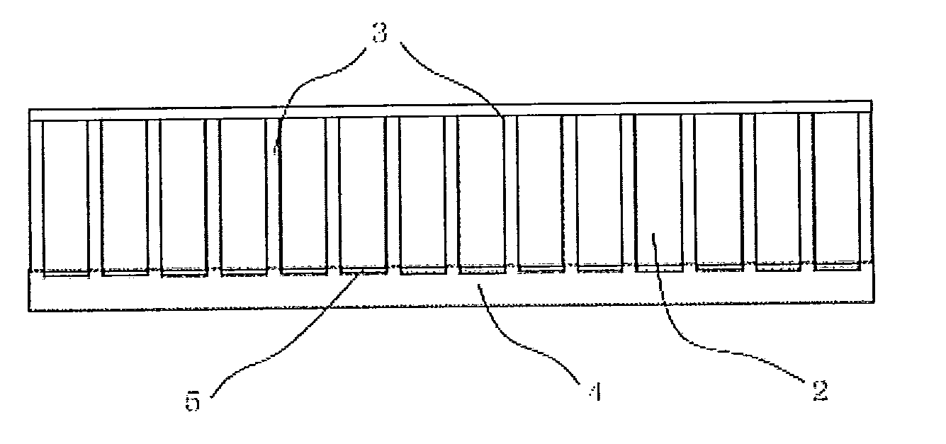
[0165]In the thirds embodiment, the above fluorescent material is used as a scintillator. The third embodiment relates to a radiation detector having this scintillator and a light receiving element. This element is designed to detect fluorescent light emitted from the scintillator. This radiation detector is preferably mounted in a medical observation device or a medical inspection device such as an X-ray CT (Computed Tomography) scanner, a PET (Positron Emission Tomography) scanner, or a PET / CT scanner.

[0166]If the above material is used as a scintillator, the problems of a decreased X-ray sensitivity, of X-ray leakage, etc., may be solved. Thus, a high-sensitivity radiation detector may be obtained.

[0167]As shown in FIGS. 22 and 23, this radiation detector may be designed to include a scintillator and a photodetector. The detector serves to detect fluorescent light emitted from this fluorescent material. FIG. 22 is a schematic perspective view of a radiation detector. FIG. 23 is a...


PUM

PropertyMeasurementUnit
wavelength rangeaaaaaaaaaa

Abstract

A fluorescent material for a scintillator to be used in a radiation detector is provided. The fluorescent material is designed to have a high fluorescent intensity and a low level of afterglow a short term of 1 to 300 ms after the termination of X-ray radiation.The above fluorescent material contains Ce as an activator. In addition, the material must contain at least Gd, Al, Ga, O, Fe, and a component M. The component M is at least one of Mg, Ti, and Ni. In addition, the composition of the material must be expressed by the general formula:(Gd1-x-zLuxCez)3+a(Al1-u-sGauScs)5−aO12 wherein 0≦a≦0.15, 0≦x≦0.5, 0.0003≦z≦0.0167, 0.2≦u≦0.6, and 0≦s≦0.1, and wherein, regarding the concentrations of Fe and M, Fe: 0.05≦Fe concentration (mass ppm)≦1, and 0≦M concentration (mass ppm)≦50.

Description

TECHNICAL FIELD[0001]The present invention relates to a fluorescent material configured to absorb radiation such as X-rays and emit fluorescence. The present invention also relates to a scintillator using such a fluorescent material. The present invention also relates to a radiation detector using such a fluorescent material.BACKGROUND ART[0002]One example of an X-ray diagnostic device is an X-ray CT (Computed Tomography) scanner. This CT scanner is composed of an X-ray tube and an X-ray detector. The tube is designed to emit a fan-shaped beam of X-rays, i.e., an X-ray fan beam. The detector is composed of many X-ray detecting elements arrayed side-by-side. The scanner operates as follows: The X-ray tube emits a series of X-ray fan beams one after another onto the X-ray detector. Each fan beam incident on the surface a tomographic layer is oriented at a predetermined angle, for example, 1 degree, from the previous one. The scanner collects thereby data on absorptions of X-rays. Subs...

Claims


Application Information

Patent Timeline
Patent Type & Authority Applications(United States)
IPC IPC(8): C09K11/80G01T1/202G01T1/20
CPCC01F17/0018G21K2004/06C01G15/006C04B35/01C04B35/44C04B35/6261C04B35/6455C04B2235/3206C04B2235/3224C04B2235/3229C04B2235/3232C04B2235/3272C04B2235/3279C04B2235/3286C04B2235/5436C04B2235/5445C04B2235/608C04B2235/661C04B2235/725C04B2235/764C04B2235/77C09K11/7774G01T1/20G21K4/00C01G15/00C01F17/32
Inventor NAKAMURA, RYOUHEIUEDA, SHUNSUKE
Owner HITACHI METALS LTD
Why Eureka
Try Eureka