Two terminal light emitting and lasing devices and methods

a technology of light-emitting and lasing devices, which is applied in the direction of lasers, semiconductor devices, semiconductor lasers, etc., can solve the problems of increasing bulky consumer products, increasing design complexity, and increasing cost and power consumption of vcsel-based optical solutions, so as to reduce the cost of lithography, and reduce the cost of manufacturing and packaging

Inactive Publication Date: 2010-08-12
THE BOARD OF TRUSTEES OF THE UNIV OF ILLINOIS +1
View PDF18 Cites 35 Cited by
  • Summary
  • Abstract
  • Description
  • Claims
  • Application Information

AI Technical Summary

Benefits of technology

[0018]The two-terminal devices of the present invention retain the fast transistor base transport mechanism of LETs and TLs while allowing the device to be compatible with existing diode circuitries and manufacturing facilities As a two

Problems solved by technology

However, the increasing higher data speed, now approaching ˜6.8 Gbps/channel for the new HDMI 1.4 standard, adds design, technical and manufacturing complexity on the traditional transmission media via copper wire.
The results are consumer products that are increasingly bulkier, unaesthetic and inflexible.
At distances of less than 5 meters, where the bulk of the consumer market is, VCSEL (vertical cavity surface emitting lasers) based optical solutions are unable to compete ba

Method used


Image

  • Two terminal light emitting and lasing devices and methods
  • Two terminal light emitting and lasing devices and methods
  • Two terminal light emitting and lasing devices and methods

Examples


Embodiment Construction

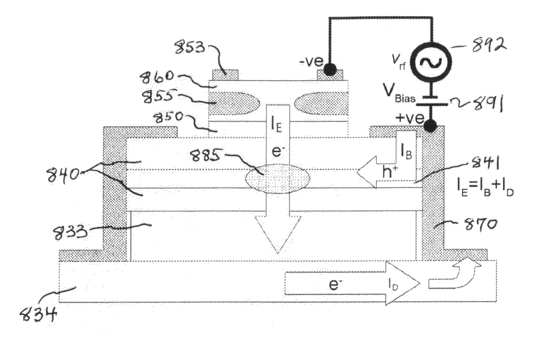
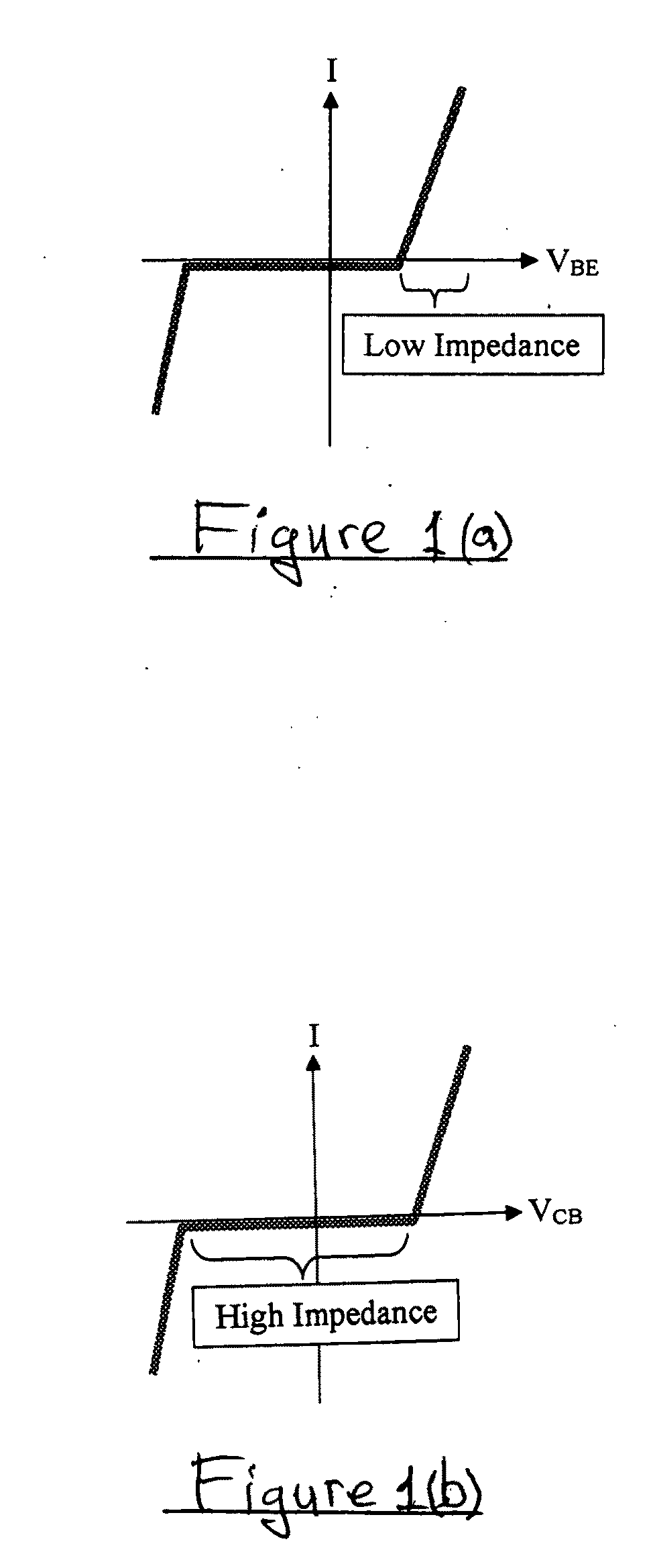
[0031]Applicant has determined that the intrinsic fast operation of the light emitting transistor or transistor laser can still be maintained in a two terminal device (single electrical input port device) by replacing the collector junction with a drain. The drain serves the same purpose of allowing excess electrons to exit the N-P (Emitter-Base) junction of the device. However, it eliminates the functionality of this excess current (since it is no longer excess current to be collected but rather eliminated) by draining the electrons towards non-radiative recombination at the common contact. The drain is required to operate at high impedance mode, which can be achieved by having a common bias with the P-terminal of the base.

[0032]Referring to FIG. 4, there as shown a device in accordance with an embodiment of the invention and which can be used in practicing an embodiment of the method of the invention. The device can be fabricated using, for example, conventional semiconductor depo...


PUM


Abstract

A method for producing light emission from a semiconductor structure, including the following steps: providing a semiconductor structure that includes a first semiconductor junction between an emitter region of a first conductivity type and a base region of a second conductivity type opposite to that of the first conductivity type, and a second semiconductor junction between the base region and a drain region; providing, within the base region, a region exhibiting quantum size effects; providing an emitter electrode coupled with the emitter region; providing a base/drain electrode coupled with the base region and the drain region; and applying signals with respect to the emitter and base/drain electrodes to obtain light emission from the semiconductor structure.

Description

PRIORITY CLAIMS[0001]Priority is claimed from U.S. Provisional Patent Application Ser. No. 61 / 204,560, filed Jan. 8, 2009, and from U.S. Provisional Patent Application Ser. No. 61 / 204,602, filed Jan. 8, 2009, and from U.S. Provisional Patent Application Ser. No. 61 / 208,422, filed Feb. 24, 2009, and all of said U.S. Provisional Patent Applications are incorporated herein by reference.RELATED APPLICATION[0002]The subject matter of this application relates to subject matter disclosed in copending U.S. patent application Ser. No. ______, filed of even date herewith and assigned to the same assignees as the present application.FIELD OF THE INVENTION[0003]This invention relates to methods and devices for producing light emission and laser emission in response to electrical signals. The invention also relates to methods and devices for producing light emission and laser emission from two terminal semiconductor devices.BACKGROUND OF THE INVENTION[0004]A part of the background hereof lies in...

Claims


Application Information

Patent Timeline
IPC IPC(8): H01S5/34H01L29/06
CPCB82Y20/00H01S5/06203H01S5/34313H01S5/3412H01S5/18311
Inventor WALTER, GABRIELFENG, MILTONHOLONYAK, JR., NICK
Owner THE BOARD OF TRUSTEES OF THE UNIV OF ILLINOIS
Why Eureka
Try Eureka