Method for producing light-emitting diode

a technology of light-emitting diodes and diodes, which is applied in the direction of semiconductor/solid-state device manufacturing, electrical equipment, semiconductor devices, etc., can solve the problems of chip heat up, chip deterioration, and many problems of conventional elements using sapphire as a substrate, so as to prevent the deterioration of current-voltage characteristics

Active Publication Date: 2010-08-12
TOYODA GOSEI CO LTD
View PDF9 Cites 140 Cited by
  • Summary
  • Abstract
  • Description
  • Claims
  • Application Information

AI Technical Summary

Benefits of technology

[0012]By providing a plating layer, the present invention is able to realize an upper-lower electrode structure and resolve the problem of heat dissipation. Further, the present invention does not require an a...

Problems solved by technology

However, conventional elements having face-up structure or flip-chip structure that use sapphire as a substrate have numerous problems.
Firstly, because the p-type electrode and the n-type electrode are aligned horizontally, the electric current flows in a horizontal direction, and as a result, the current density tends to increase in localized areas, causing t...

Method used


Image

  • Method for producing light-emitting diode
  • Method for producing light-emitting diode
  • Method for producing light-emitting diode

Examples


example 1

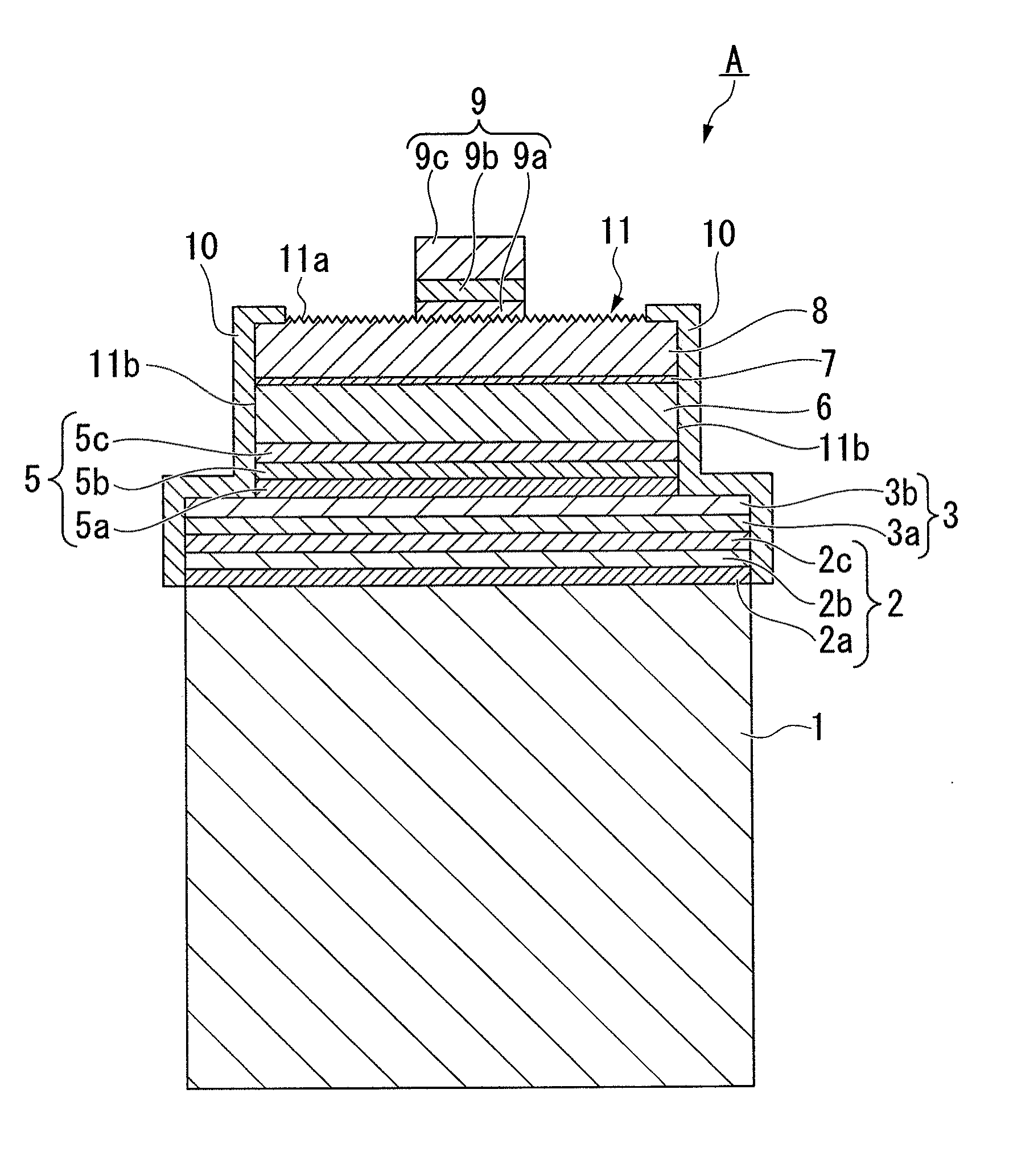
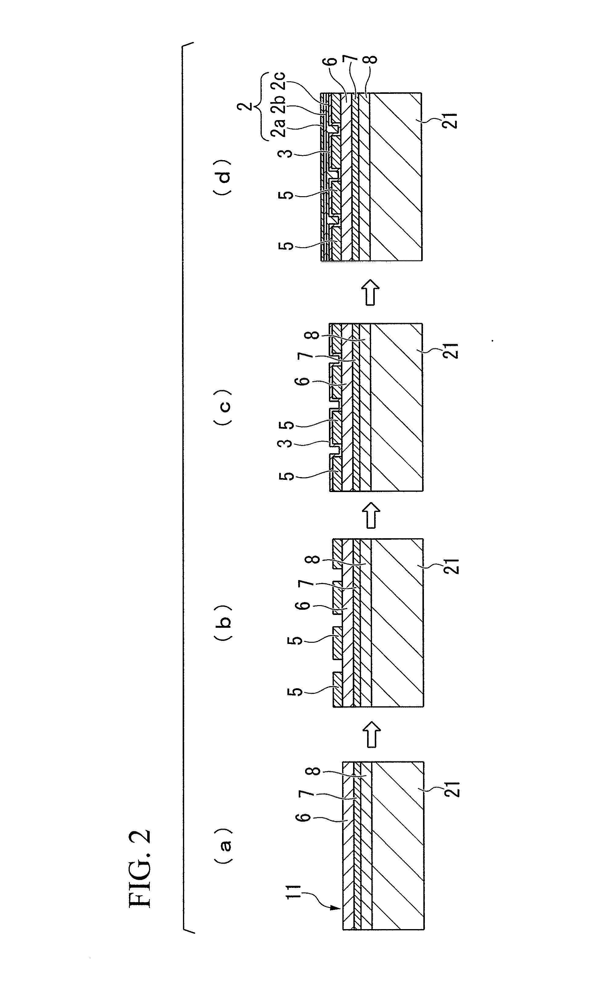
[0125]A light-emitting diode A illustrated in FIG. 1 was prepared in the manner described below.

[0126]Namely, a buffer layer of thickness 40 nm composed of AlN was formed on a substrate composed of sapphire, and an undoped GaN underlayer of thickness 2 μm, a Si-doped n-type GaN contact layer of thickness 2 μm and an n-type In0.1Ga0.9N cladding layer of thickness 20 nm (the n-type semiconductor layer), a light-emitting layer having a multiple quantum well structure in which a Si-doped GaN barrier layer of thickness 15 nm and an In0.2Ga0.8N well layer of thickness 2 nm were laminated 5 times and finally provided with a barrier layer, and a Mg-doped p-type Al0.1Ga0.9N cladding layer of thickness 10 nm and a Mg-doped p-type Al0.02Ga0.98N contact layer of thickness 200 nm (the p-type semiconductor layer) were laminated sequentially onto the buffer layer, yielding a laminated semiconductor layer.

[0127]Subsequently, an ohmic contact layer of thickness 2 nm, a reflective layer of thickness ...


PUM


Abstract

The present invention provides a method for producing a light-emitting diode, the method comprising a lamination step of forming a laminated semiconductor layer by sequentially laminating an n-type semiconductor layer, a light-emitting layer and a p-type semiconductor layer onto a substrate, as well as forming a plurality of reflective p-type electrodes on top of the p-type semiconductor layer, a plating step of forming a seed layer that covers the reflective p-type electrodes and the p-type semiconductor layer, and fowling a plating layer on top of the seed layer, a removal step of removing the substrate from the n-type semiconductor layer, thereby exposing a light extraction surface of the n-type semiconductor layer, and an electrode formation step of performing dry etching of the light extraction surface of the n-type semiconductor layer using an etching gas containing the same element as a dopant element within the n-type semiconductor layer, and subsequently forming an n-type electrode on the light extraction surface.

Description

TECHNICAL FIELD[0001]The present invention relates to a method for producing a light-emitting diode.[0002]Priority is claimed on Japanese Patent Application No. 2007-171920, filed Jun. 29, 2007, the content of which is incorporated herein by reference.BACKGROUND ART[0003]Group-III nitride semiconductors have a direct transition-type band gap at energy levels corresponding with a range from visible light to the ultraviolet light region and also exhibit excellent light emission efficiency, and have therefore been widely commercialized as semiconductor light-emitting elements such as light-emitting diodes (LED) and laser diodes (LD) for use in all manner of applications. Further, even when used within electronic devices, group-III nitride semiconductors have the potential to yield superior properties to those obtainable using conventional group III-V compound semiconductors.[0004]Generally, group-III nitride semiconductors are produced by a metal-organic chemical vapor deposition (MOCV...

Claims


Application Information

Patent Timeline
IPC IPC(8): H01L33/00H01L33/22H01L33/40H01L33/44H01L33/46
CPCH01L33/0079H01L33/44H01L33/405H01L33/0095H01L33/0093
Inventor HODOTA, TAKASHI
Owner TOYODA GOSEI CO LTD
Why Eureka
Try Eureka