Method for producing light-emitting diode

a technology of light-emitting diodes and diodes, which is applied in the direction of basic electric elements, electrical equipment, semiconductor devices, etc., can solve the problems of chip heat up, chip deterioration, and many problems of conventional elements using sapphire as a substrate, so as to prevent the deterioration of current-voltage characteristics

Active Publication Date: 2012-01-17
TOYODA GOSEI CO LTD
View PDF18 Cites 10 Cited by
  • Summary
  • Abstract
  • Description
  • Claims
  • Application Information

AI Technical Summary

Benefits of technology

[0019]By providing a plating layer, the present invention is able to realize an upper-lower electrode structure and resolve the problem of heat dissipation. Further, the present invention does not require an annealing treatment during formation of the ohmic electrode, and therefore degradation of the ohmic electrode within the light-emitting diode and deterioration in the current-voltage characteristics can be prevented.

Problems solved by technology

However, conventional elements having face-up structure or flip-chip structure that use sapphire as a substrate have numerous problems.
Firstly, because the p-type electrode and the n-type electrode are aligned horizontally, the electric current flows in a horizontal direction, and as a result, the current density tends to increase in localized areas, causing the chip to heat up.
Secondly, because the sapphire that is used as the substrate is extremely hard and does not exhibit cleavability, high level technology is required to generate the chips.
Thirdly, the thermal conductivity of sapphire is comparatively low, and therefore the heat generated in the group-III nitride semiconductor layer cannot be dissipated efficiently.

Method used


Image

  • Method for producing light-emitting diode
  • Method for producing light-emitting diode
  • Method for producing light-emitting diode

Examples


example 1

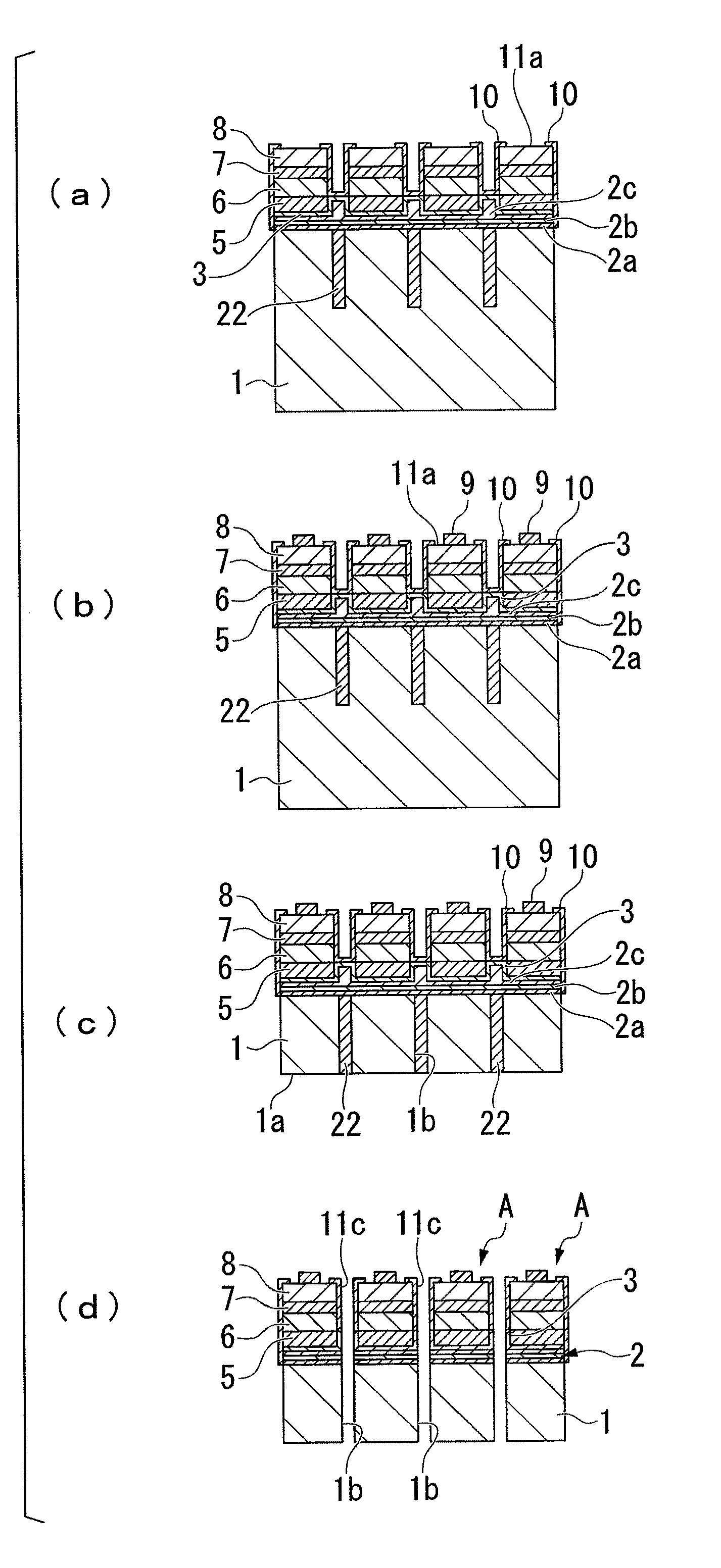
[0132]A light-emitting diode A illustrated in FIG. 1 was prepared in the manner described below.

[0133]Namely, a buffer layer of thickness 40 nm composed of AlN was formed on a substrate composed of sapphire, and an undoped GaN underlayer of thickness 2 μm, a Si-doped n-type GaN contact layer of thickness 2 μm and an n-type In0.1Ga0.9N cladding layer of thickness 20 nm (the n-type semiconductor layer), a light-emitting layer having a multiple quantum well structure in which a Si-doped GaN barrier layer of thickness 15 nm and an In0.2Ga0.8N well layer of thickness 2 nm were laminated 5 times and finally provided with a barrier layer, and a Mg-doped p-type Al0.1Ga0.9N cladding layer of thickness 10 nm and a Mg-doped p-type Al0.02Ga0.98N contact layer of thickness 200 nm (the p-type semiconductor layer) were laminated sequentially onto the buffer layer, yielding a laminated semiconductor layer.

[0134]Subsequently, an ohmic contact layer of thickness 2 nm, a reflective layer of thickness ...


PUM


Abstract

The present invention provides a method for producing a light-emitting diode, the method comprising a lamination step of forming a laminated semiconductor layer by sequentially laminating an n-type semiconductor layer, a light-emitting layer and a p-type semiconductor layer onto a substrate, as well as forming a plurality of reflective p-type electrodes on top of the p-type semiconductor layer, a plating step of forming a seed layer that covers the reflective p-type electrodes and the p-type semiconductor layer, and fowling a plating layer on top of the seed layer, a removal step of removing the substrate from the n-type semiconductor layer, thereby exposing a light extraction surface of the n-type semiconductor layer, and an electrode formation step of performing dry etching of the light extraction surface of the n-type semiconductor layer using an etching gas containing the same element as a dopant element within the n-type semiconductor layer, and subsequently forming an n-type electrode on the light extraction surface.

Description

TECHNICAL FIELD[0001]The present invention relates to a method for producing a light-emitting diode.[0002]Priority is claimed on Japanese Patent Application No. 2007-171920, filed Jun. 29, 2007, the content of which is incorporated herein by reference.BACKGROUND ART[0003]Group-III nitride semiconductors have a direct transition-type band gap at energy levels corresponding with a range from visible light to the ultraviolet light region and also exhibit excellent light emission efficiency, and have therefore been widely commercialized as semiconductor light-emitting elements such as light-emitting diodes (LED) and laser diodes (LD) for use in all manner of applications. Further, even when used within electronic devices, group-III nitride semiconductors have the potential to yield superior properties to those obtainable using conventional group III-V compound semiconductors.[0004]Generally, group-III nitride semiconductors are produced by a metal-organic chemical vapor deposition (MOCV...

Claims


Application Information

Patent Timeline
Patent Type & Authority Patents(United States)
IPC IPC(8): H01L21/00H01L33/00H01L33/40H01L33/44
CPCH01L33/0079H01L33/405H01L33/0095H01L33/44H01L33/0093
Inventor HODOTA, TAKASHI
Owner TOYODA GOSEI CO LTD
Why Eureka
Try Eureka