Nitride semiconductor light emitting device and method of manufacturing the same

a technology of semiconductor light emitting device and semiconductor, which is applied in the direction of semiconductor/solid-state device manufacturing, semiconductor devices, semiconductor devices, etc., can solve the problems of excessive external efficiency and high electrical discharge of semiconductor light emitting devices, and achieve high light extraction efficiency and resistance to electrostatic discharg

Inactive Publication Date: 2010-08-19
SAMSUNG ELECTRONICS CO LTD
View PDF14 Cites 38 Cited by
  • Summary
  • Abstract
  • Description
  • Claims
  • Application Information

AI Technical Summary

Benefits of technology

[0009]An aspect of the present invention provides a nitride semiconductor light emitting device which achieves high resistance to electrostatic discharge (ESD) and high light extraction efficiency.

Problems solved by technology

Here, the internal quantum efficiency reaches almost 100%, however the quantum external efficiency is excessively low.
Also, semiconductor light emitting devices are susceptible to electrostatic discharge (ESD), which is easily generated in people or objects.

Method used


Image

  • Nitride semiconductor light emitting device and method of manufacturing the same
  • Nitride semiconductor light emitting device and method of manufacturing the same
  • Nitride semiconductor light emitting device and method of manufacturing the same

Examples


Embodiment Construction

[0032]Exemplary embodiments of the present invention will now be described in detail with reference to the accompanying drawings. The invention may, however, be embodied in many different forms and should not be construed as limited to the embodiments set forth herein. Rather, these embodiments are provided so that this disclosure will be thorough and complete, and will fully convey the scope of the invention to those skilled in the art. In the drawings, the shapes and dimensions of elements may be exaggerated for clarity. Like reference numerals in the drawings denote like elements, and thus their description will be omitted.

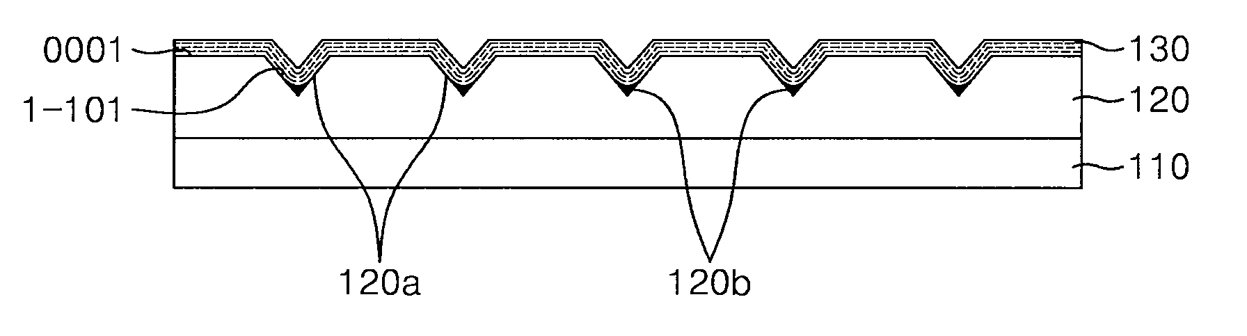
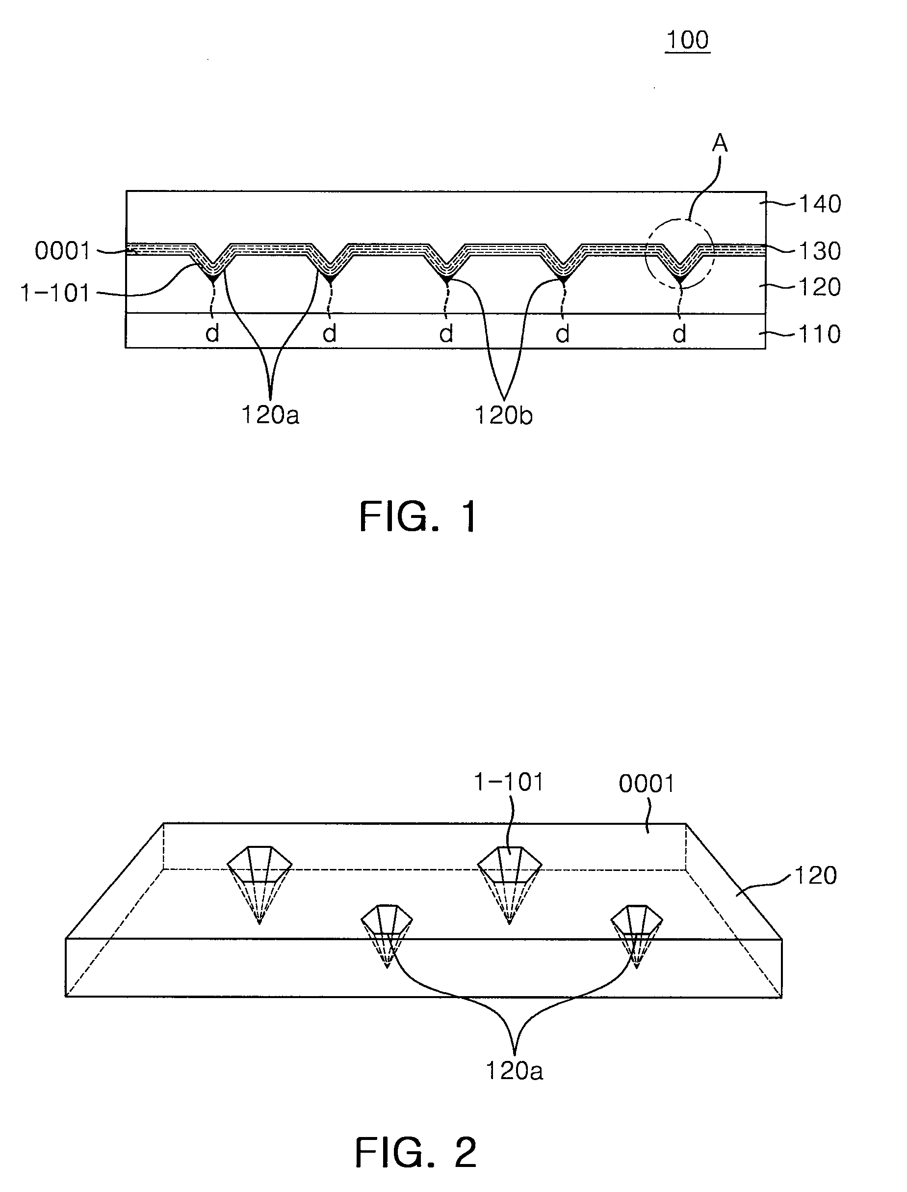
[0033]FIG. 1 is a cross-sectional view showing a nitride semiconductor light emitting device according to an exemplary embodiment of the present invention. Referring to FIG. 1, a nitride semiconductor light emitting device 100 includes a substrate 110; a first conductivity type nitride semiconductor layer 120 disposed on the substrate 110 and including a plural...


PUM


Abstract

A nitride semiconductor light emitting device includes a substrate, a first conductivity type nitride semiconductor layer disposed on the substrate and including a plurality of V-pits placed in a top surface thereof, a silicon compound formed in the vertex region of each of the V-pits, an active layer disposed on the first conductivity type nitride semiconductor layer and including depressions conforming to the shape of the plurality of V-pits, and a second conductivity type nitride semiconductor layer disposed on the active layer. The nitride semiconductor light emitting device, when receiving static electricity achieves high resistance to electrostatic discharge (ESD) since current is concentrated in the V-pits and the silicon compound placed on dislocations caused by lattice defects.

Description

CROSS-REFERENCE TO RELATED APPLICATIONS[0001]This application claims the priority of Korean Patent Application No. 10-2009-0012994 filed on Feb. 17, 2009, in the Korean Intellectual Property Office, the disclosure of which is incorporated herein by reference.BACKGROUND OF THE INVENTION[0002]1. Field of the Invention[0003]The present invention relates to a semiconductor light emitting device and a method of manufacturing the same, and more particularly, to a nitride semiconductor light emitting device and a method of manufacturing the same, which can achieve high resistance to electrostatic discharge (ESD), and high light extraction efficiency.[0004]2. Description of the Related Art[0005]Light emitting diodes (LEDs), as one type of semiconductor light emitting device, generate light of various colors by electron-hole recombination occurring at a p-n junction when current is applied. LEDs are greatly advantageous over filament-based light emitting devices. That is, LEDs have a longer ...

Claims


Application Information

Patent Timeline
Patent Type & Authority Applications(United States)
IPC IPC(8): H01L33/00H01L21/30
CPCH01L33/18H01L33/32H01L33/20
Inventor OH, JEONG TAKKIM, YONG CHUNKIM, DONG JOONLEE, DONG JU
Owner SAMSUNG ELECTRONICS CO LTD
Why Eureka
Try Eureka