

Transistor, semiconductor device including the transistor, and manufacturing method of the transistor and the semiconductor device
a manufacturing method and semiconductor technology, applied in the direction of transistors, semiconductor devices, electrical apparatus, etc., can solve the problems of deterioration of electrical characteristics of elements, problems of variation, and likely variation of semiconductor characteristics, so as to suppress the effect of transistor variation in characteristics
- Summary
- Abstract
- Description
- Claims
- Application Information
AI Technical Summary
Benefits of technology
Problems solved by technology
Method used
Image

Examples
embodiment 1
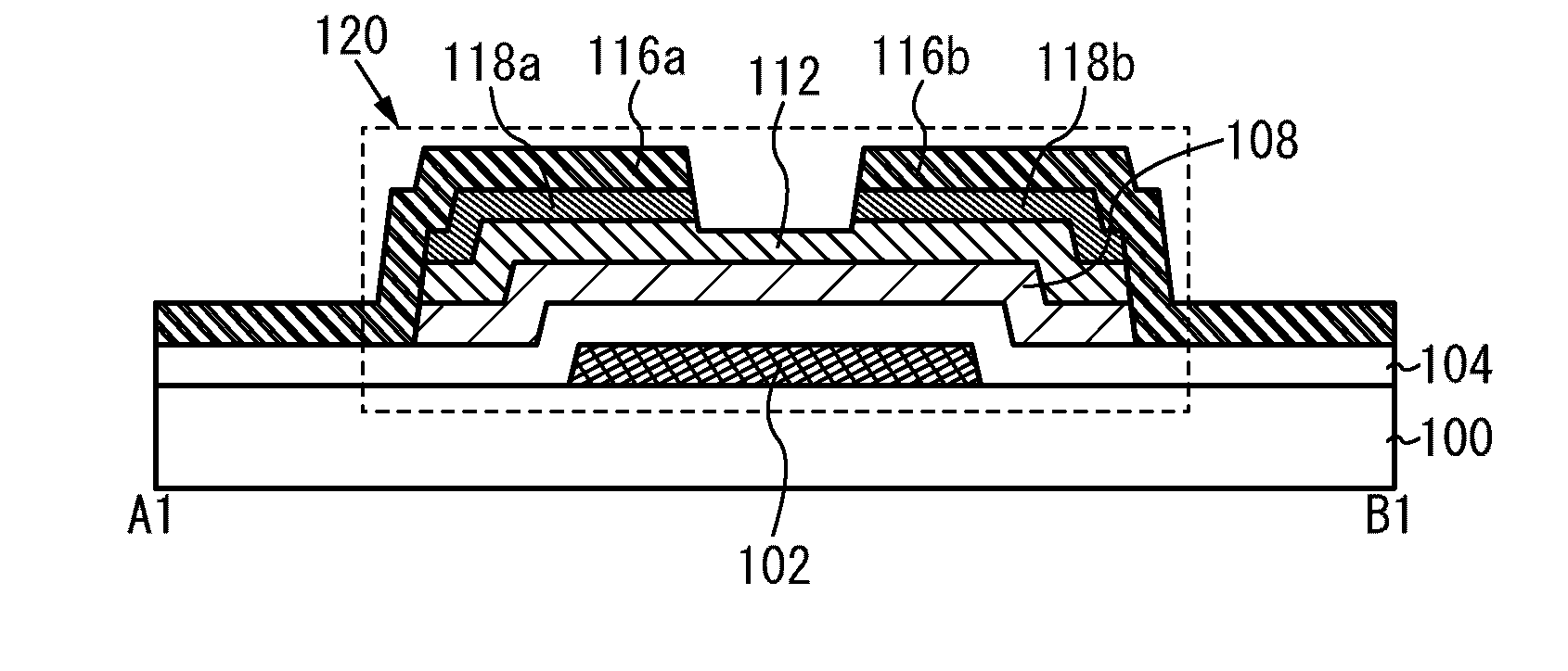
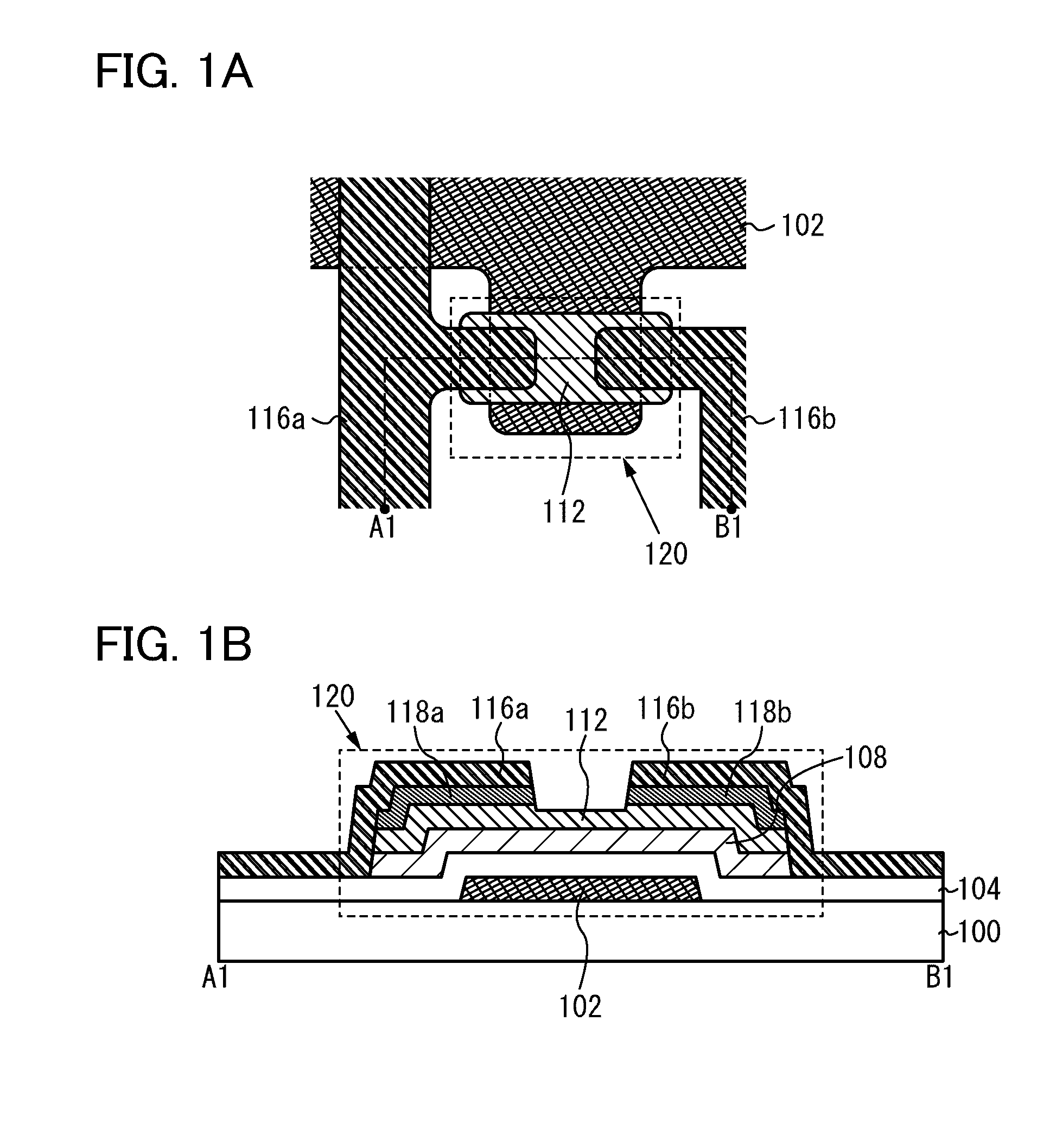
[0053]In this embodiment, an example of a structure of a transistor included in a semiconductor device will be described with reference to the drawings.
[0054]A transistor 120 illustrated in FIGS. 1A and 1B includes a gate (including a gate wiring and a gate electrode (hereinafter referred to as a “gate electrode 102”)) provided over a substrate 100, a gate insulating layer 104 provided over the gate electrode 102, an oxide semiconductor layer 108 provided over the gate insulating layer 104, a silicon layer 112 provided in contact with a surface of the oxide semiconductor layer 108, a first impurity semiconductor layer 118a and a second impurity semiconductor layer 118b provided over the silicon layer 112, a source (including a source wiring and a source electrode (hereinafter referred to as a “source electrode layer 116a”)) electrically connected to the first impurity semiconductor layer 118a, and a drain (including a drain wiring and a drain electrode (also referred to as a “drain ...
embodiment 2
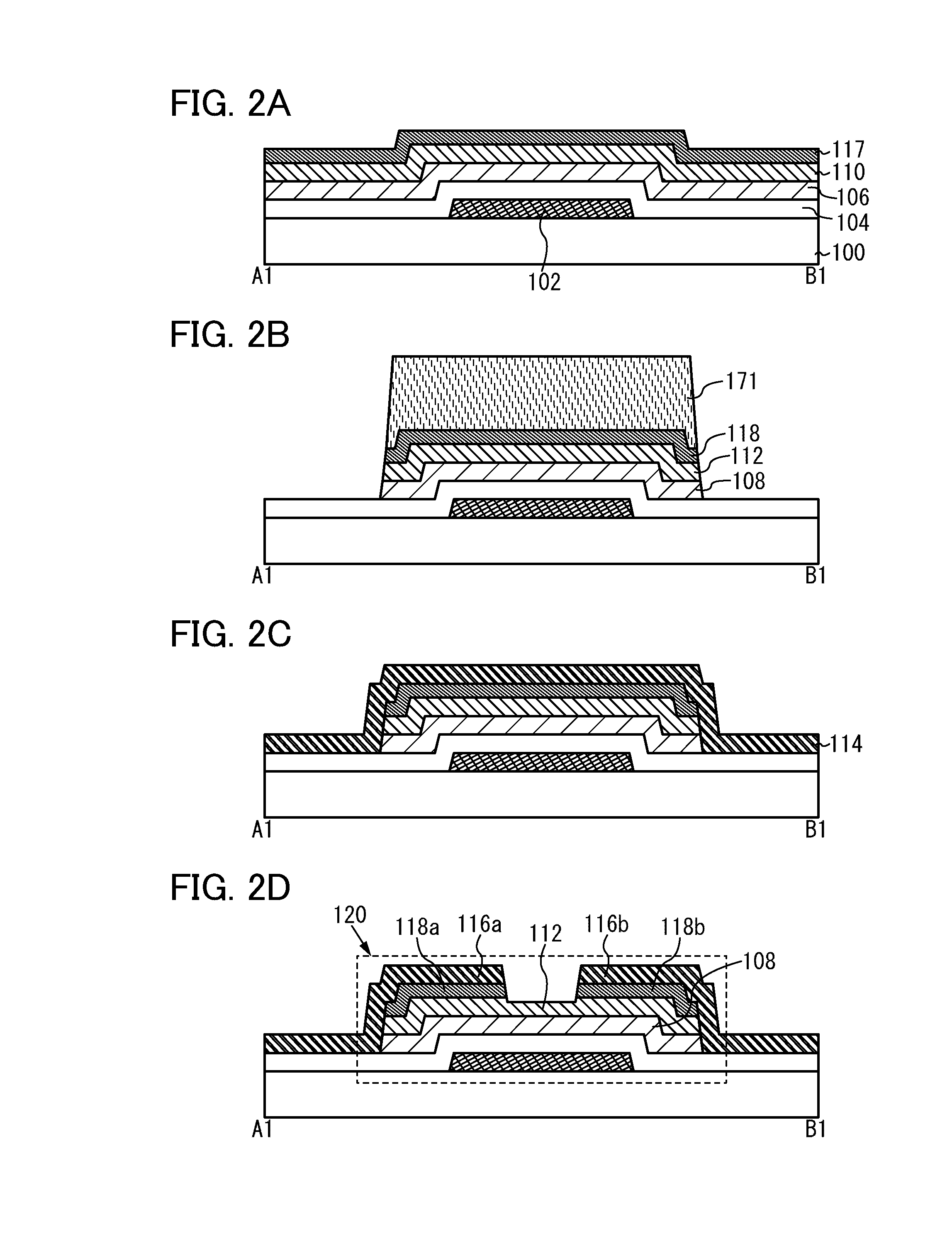
[0115]In this embodiment, a structure and a manufacturing method of a transistor which are different from those of Embodiment 1 will be described with reference to the drawings.
[0116]First, the manufacturing method of the transistor will be described with reference to FIGS. 6A to 6E. Note that the manufacturing process (such as applicable materials) described in this embodiment is in common with that of Embodiment 1 in many points. Thus, description of the common points are omitted below and only points different from those of Embodiment 1 will be described in detail.
[0117]First, a gate electrode 102 is formed over a substrate 100, and then a gate insulating layer 104, an oxide semiconductor layer 106, and a silicon layer 110 are sequentially formed to be stacked over the gate electrode 102 (see FIG. 6A).
[0118]Next, the oxide semiconductor layer 106 and the silicon layer 110 are etched to form an island-shaped oxide semiconductor layer 108 and an island-shaped silicon layer 112 (see...
embodiment 3
[0127]In this embodiment, a manufacturing process of a display device which is an example of a usage pattern of a semiconductor device including the transistor described in Embodiment 1 or 2 will be described with reference to the drawings. Note that the manufacturing process (such as applicable materials) described in this embodiment is in common with that of Embodiment 1 in many points. Thus, description of the common points are omitted below and only points different from those of Embodiment 1 will be described in detail. In the description below, FIGS. 8A to 8C and FIGS. 9A to 9C are cross-sectional views, and FIG. 10, FIG. 11, FIG. 12, and FIG. 13 are top views.
[0128]First, wirings and electrodes (a gate wiring including the gate electrode 102, a capacitor wiring 308, and a first terminal 321) are formed over the substrate 100 having an insulating surface, and then the gate insulating layer 104, the oxide semiconductor layer 106, the silicon layer 110, and the impurity semicond...
PUM
 Abstract
Description
Claims
Application Information