Display device with chiplet drivers

a chiplet driver and display device technology, applied in the field of display devices, can solve the problems of flicker perceptible, the current necessary to drive an entire row (or column) in the display, and the limitation of the number of rows (or columns) of the passive-matrix drive devi

Active Publication Date: 2010-08-19
GLOBAL OLED TECH
View PDF28 Cites 42 Cited by
  • Summary
  • Abstract
  • Description
  • Claims
  • Application Information

AI Technical Summary

Benefits of technology

[0015]The present invention has the advantage that, by providing a display device with chiplet drivers having row and column electrode connections, the number of connection pads and the size and number of chiplets are reduced. In an embodiment of the present invention, a plurality of arrays provides reduced flicker and power requirements. Another advantage of the present invention is that, by providing large spaces on the display substrate for wiring, larger wires can be employed at lower cost and with higher electrical performance. A further advantage is that the monocrystalline silicon chiplets have high mobility and uniformity.
is that, by providing large spaces on the display substrate for wiring, larger wires can be employed at lower cost and with higher electrical performance. A further advantage is that the monocrystalline silicon chiplets have high mobility and uniformity.

Problems solved by technology

However, a passive-matrix drive device is limited in the number of rows (or columns) that can be included in the device since the sequential nature of the row (or column) driving creates flicker.
If too many rows are included, the flicker can become perceptible.
Moreover, the currents necessary to drive an entire row (or column) in a display can be problematic and the power required for the non-imaging pre-charge and discharge steps of PM driving become dominant as the area of the PM display grows.
These two problems limit the physical size of a passive-matrix display.
Thin-film transistors (TFTs) made from amorphous or polycrystalline silicon are relatively large and have lower performance compared to conventional transistors made in crystalline silicon wafers.
Moreover, such thin-film devices typically exhibit local or large-area non-uniformity across the glass substrate that results in non-uniformity in the electrical performance and visual appearance of display employing such materials.
Since a conventional passive-matrix display design is limited in size and number of light-emitting elements, and an active-matrix design using TFTs has lower electrical performance, there is a need for improved control for display devices employing LEDs that overcomes these problems.

Method used


Image

  • Display device with chiplet drivers
  • Display device with chiplet drivers
  • Display device with chiplet drivers

Examples


Embodiment Construction

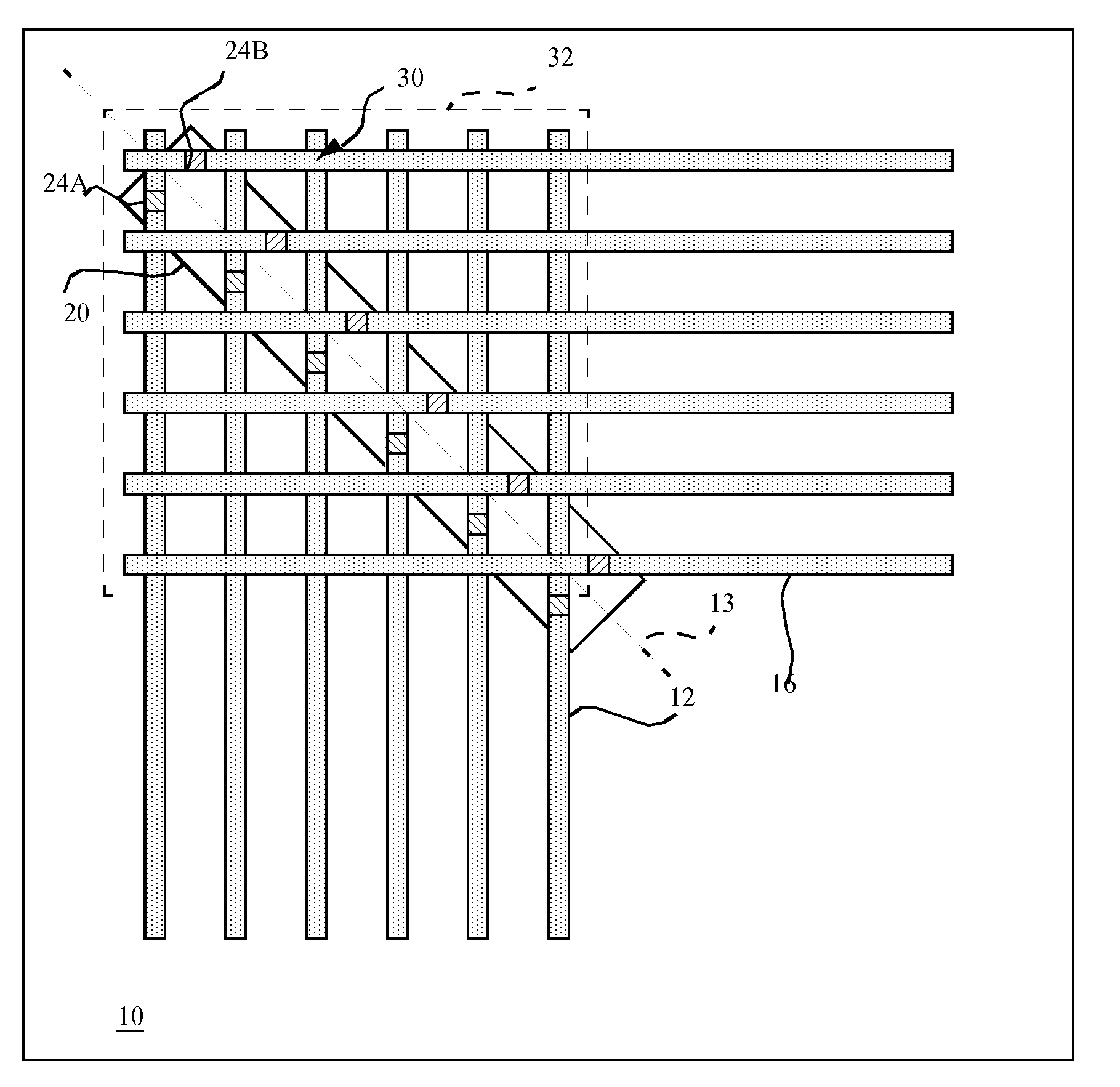
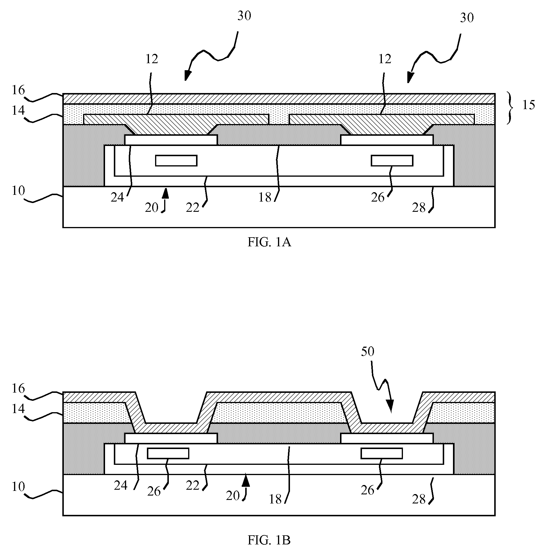
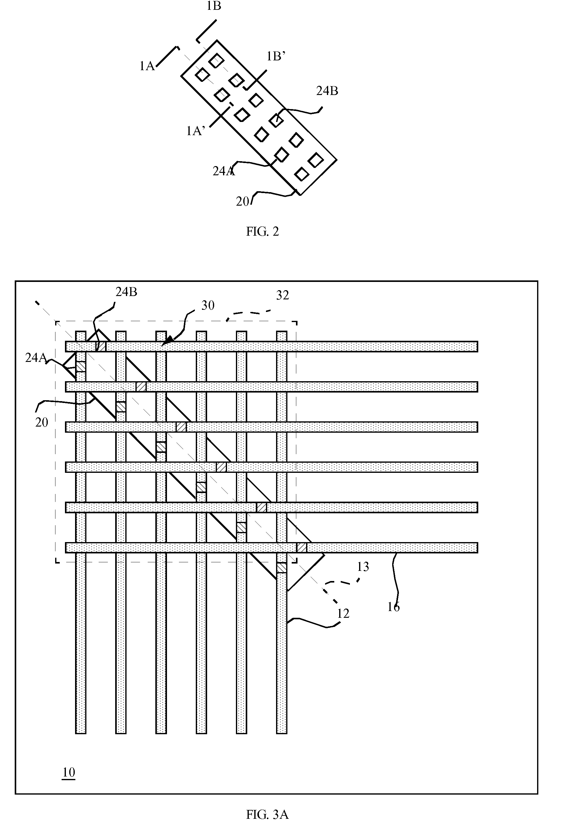
[0033]Referring to FIG. 3A, in one embodiment, the present invention includes a display device including a substrate 10, a first layer having an array of row electrodes 16 formed in rows across the substrate 10 in a first direction and a second layer having an array of column electrodes 12 formed in columns across the substrate 10 in a second direction different from the first direction and wherein the first and second electrodes overlap to form pixel locations 30. Referring also to FIG. 1A, one or more layers 14 of light-emitting material are formed between the row and column electrodes 16, 12. Light-emitting diodes 15 are pixels 30 that form a two-dimensional array 32 of pixels in the pixel locations and emit light when a current is passed through the light-emitting layer 14 from the row and column electrodes 16, 12. A plurality of chiplets 20 are located over the substrate 10, the number of chiplets 20 being less than the number of pixels 30, each chiplet 20 exclusively controlli...


PUM


Abstract

A display device, including a substrate; a first layer having an array of row electrodes formed in rows across the substrate in a first direction and a second layer having an array of column electrodes formed in columns across the substrate in a second direction different from the first direction wherein the row and column electrodes overlap to form pixel locations; one or more layers of light-emitting material formed between the row and column electrodes to form a two-dimensional array of pixels, the pixels being located in the pixel locations; and a plurality of chiplets located over the substrate, the number of chiplets being less than the number of pixels, each chiplet exclusively controlling a subset of row electrodes and a subset of column electrodes, whereby the pixels are controlled to display an image.

Description

FIELD OF THE INVENTION[0001]The present invention relates to display devices having a substrate with distributed, independent chiplets for controlling a pixel array.BACKGROUND OF THE INVENTION[0002]Flat-panel display devices are widely used in conjunction with computing devices, in portable devices, and for entertainment devices such as televisions. Such displays typically employ a plurality of pixels distributed over a substrate to display images. Each pixel incorporates several, differently colored light-emitting elements commonly referred to as sub-pixels, typically emitting red, green, and blue light, to represent each image element. As used herein, pixels can refer to a single light-emitting element or a group of differently colored light-emitting elements. A variety of flat-panel display technologies are known, for example plasma displays, liquid crystal displays, and light-emitting diode (LED) displays.[0003]Light emitting diodes (LEDs) incorporating thin films of light-emitt...

Claims


Application Information

Patent Timeline
Patent Type & Authority Applications(United States)
IPC IPC(8): G09G3/30G09G3/32
CPCG09G3/2088G09G3/3208G09G2300/0408H01L27/3276G09G2300/0465G09G2310/0221H01L27/3255G09G2300/0426H10K59/129H10K59/131G02F1/1345G09F9/30G09F13/22H05B33/00H05B33/20
Inventor COK, RONALD S.HAMER, JOHN W.
Owner GLOBAL OLED TECH
Why Eureka
Try Eureka