Eureka AIR delivers breakthrough ideas for toughest innovation challenges, trusted by R&D personnel around the world.

Dielectric enhancements to chip-to-chip capacitive proximity communication

a capacitive proximity and dielectric technology, applied in the direction of electrical apparatus, semiconductor devices, semiconductor/solid-state device details, etc., can solve the problems of limited ability of processors to exploit the advancement of computational power, inability of electrical signaling to drive off-chip structures efficiently, and the need for increasing the serial data rate over many communication channels, etc., to achieve high permittivity dielectric, improve signal level, and high permittivity

Active Publication Date: 2010-08-26
ORACLE INT CORP
View PDF10 Cites 6 Cited by
  • Summary
  • Abstract
  • Description
  • Claims
  • Application Information

AI Technical Summary

Benefits of technology

[0021]In general, in one aspect, the present invention relates to a method for improving signal levels between capacitively-coupled chips in PxC. The method includes the steps of depositing a high permittivity dielectric material layer over a signal pad of a first chip, and placing a second chip in close proximity to the first chip such that faces of the signal pads align to enable for capacitive signal coupling. The high permittivity dielectric material layer that fills at least a portion of a gap between the first chip and the second chip, and improves capacitive coupling between signal pads of the first chip and the second chip by providing for an increased permittivity in the gap between the first chip and the second chip. The increased permittivity ensures that electric fields are substantially confined to a space between the signal pad of the first chip and the signal pad of the second chip.
[0022]In general, in one aspect, the present invention relates to a processing unit that provides for increased signal coupling between capacitively-coupled chips. The processing unit includes a first semiconductor chip having a signal pad atop which a high permittivity dielectric material layer is deposited, and a second semiconductor chip in proximity to the first semiconductor chip such that a face of a signal pad of the second chip is aligned with a face of the signal pad of the first chip to enable for capacitive signal coupling. The face of the signal pad of the first chip is an area of deposition of the high permittivity dielectric material layer that fills at least a portion of a gap between the first chip and the second chip. The high permittivity dielectric material layer improves capacitive coupling between signal pads of the first chip and the second chip by providing for an increased permittivity in the gap between the first chip and the second chip. The increased permittivity ensures that electric fields are substantially confined to a space between the signal pad of the first chip and the signal pad of the second chip.

Problems solved by technology

With scaling of processor technology to future generational requirements, the pressing need for increased serial data rate over many communication channels to off-chip memory is not eased by the inability of electrical signaling to drive off-chip structures efficiently due to mismatch between on-chip and off-chip bandwidths.
Thus, the ability of processors to exploit advancements in computational power, clock frequency, transistor count, multi-core architectures and the like is limited.
However, an unwanted parasitic capacitance Cp may have to be factored into received signal calculations.

Method used


Image

  • Dielectric enhancements to chip-to-chip capacitive proximity communication
  • Dielectric enhancements to chip-to-chip capacitive proximity communication
  • Dielectric enhancements to chip-to-chip capacitive proximity communication

Examples


Embodiment Construction

[0031]Specific embodiments of the invention will now be described in detail with reference to the accompanying figures. Like elements in the various figures are denoted by like reference numerals for consistency.

[0032]In the following detailed description of embodiments of the invention, numerous specific details are set forth in order to provide a more thorough understanding of the invention. However, it will be apparent to one of ordinary skill in the art that the invention may be practiced without these specific details. In other instances, well-known features have not been described in detail to avoid unnecessarily complicating the description.

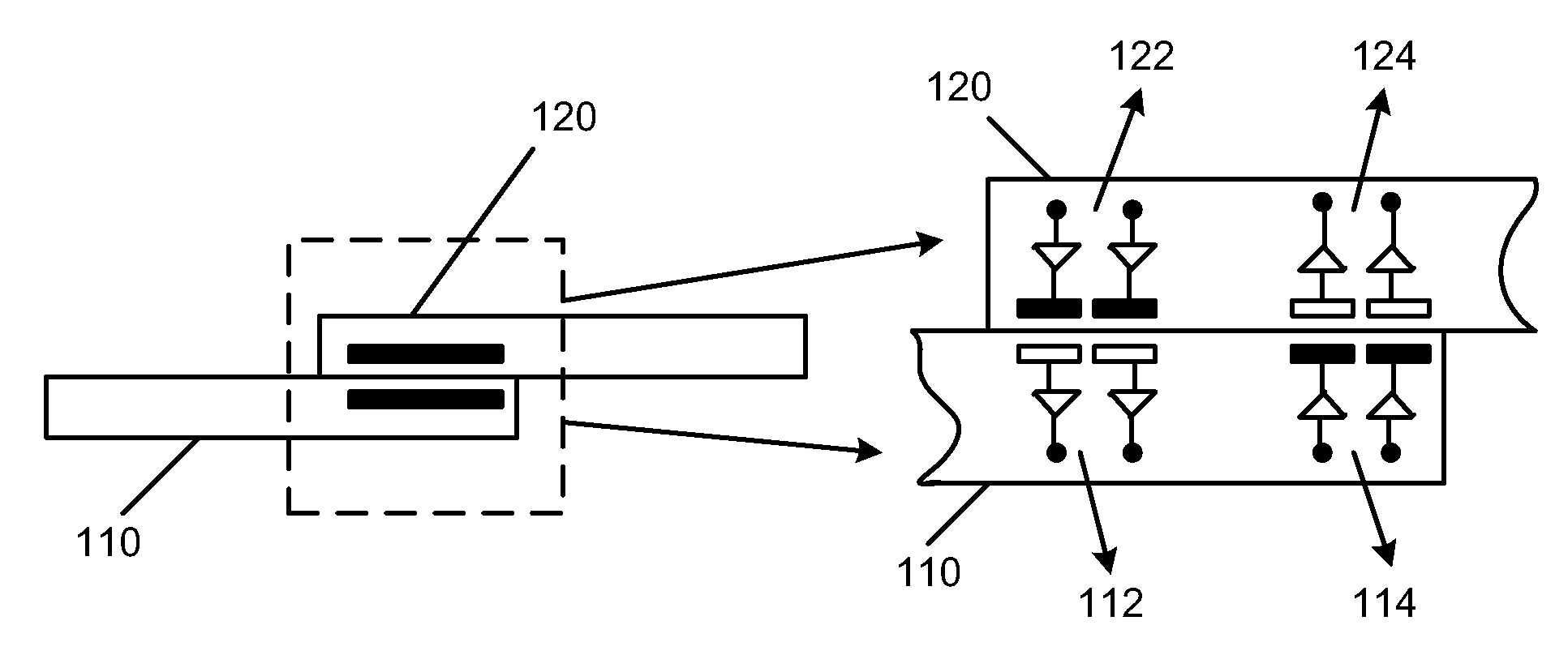
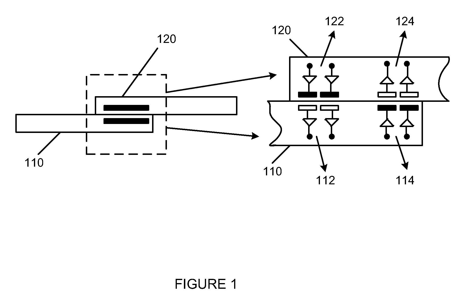
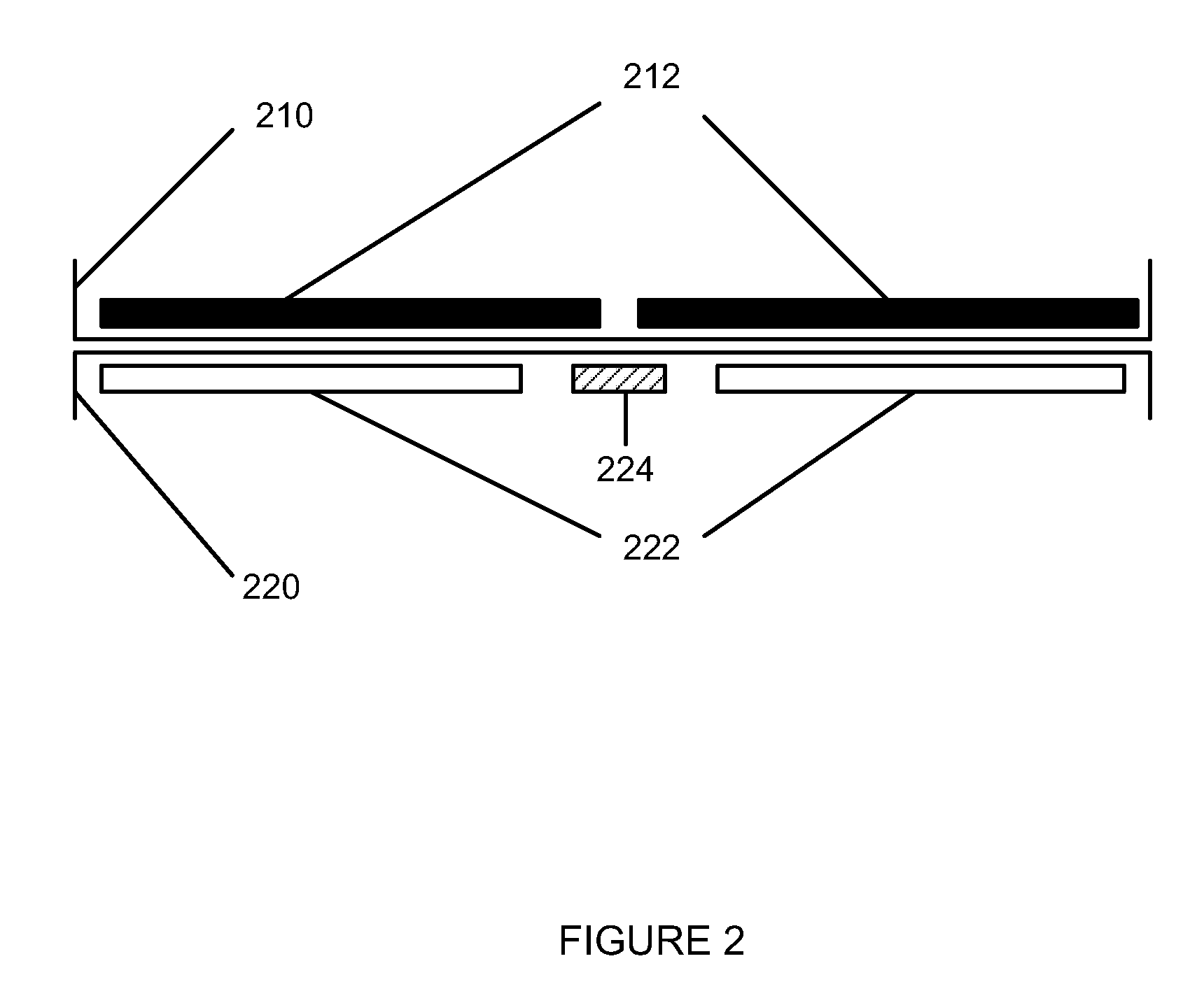
[0033]In general, embodiments of the present invention describe a specific method for increasing coupling between signal pads of chips in a PxC configuration by depositing a layer of a high permittivity dielectric material directly atop signal pads. In one or more embodiments, such a high permittivity dielectric material may provide for el...


PUM


Abstract

A method for improving signal levels between capacitively-coupled chips in proximity communication (PxC) includes depositing a high permittivity dielectric material layer over a signal pad of a first chip, and placing a second chip in close proximity to the first chip such that faces of the signal pads align to enable for capacitive signal coupling. The high permittivity dielectric material layer that fills at least a portion of a gap between the first chip and the second chip, and improves capacitive coupling between signal pads of the first chip and the second chip by providing for an increased permittivity in the gap between the first chip and the second chip. The increased permittivity ensures that electric fields are substantially confined to a space between the signal pad of the first chip and the signal pad of the second chip.

Description

BACKGROUND OF INVENTION[0001]1. Field of the Invention[0002]The present invention relates generally to a method for increasing signal coupling between pads of chips engaged in capacitive proximity communication (PxC). More specifically, the present invention relates to a method for increasing signal coupling, where a high permittivity dielectric material is directly deposited atop the pads to enable confinement of electric fields within pad gaps of the chips.[0003]2. Background Art[0004]With scaling of processor technology to future generational requirements, the pressing need for increased serial data rate over many communication channels to off-chip memory is not eased by the inability of electrical signaling to drive off-chip structures efficiently due to mismatch between on-chip and off-chip bandwidths. Thus, the ability of processors to exploit advancements in computational power, clock frequency, transistor count, multi-core architectures and the like is limited. One way to ci...

Claims


Application Information

Patent Timeline
IPC IPC(8): H01L23/29H01L21/02
CPCH01L23/66H01L25/0657H01L2225/06527H01L2924/0002H01L2924/00
Inventor KRISHNAMOORTHY, ASHOKCUNNINGHAM, JOHN E.
Owner ORACLE INT CORP
Why Eureka
Eureka Blog
Learn More