Optical interconnection assembled circuit

a technology of assembled circuits and optical wirings, applied in the direction of optical elements, instruments, optical waveguide light guides, etc., can solve the problems of optical cross-talk, difficult to say that the two-dimensional layout is efficient, etc., and achieve the effect of high density disposition of optical wirings, reduced manufacturing processes, and high flexibility

Inactive Publication Date: 2010-08-26
HITACHI LTD
View PDF7 Cites 51 Cited by
  • Summary
  • Abstract
  • Description
  • Claims
  • Application Information

AI Technical Summary

Benefits of technology

[0020]Even in the above case, because optical connections are made through the lenses provided on the semiconductor substrate of the optical elements and the mirror parts of the optical waveguide layer respectively, no optical part is required between each optical waveguide and the optical photonic device. Thus the number of parts and components, as well as the number of manufacturin

Problems solved by technology

Thus it is difficult to say that the two-dimensional layout is an efficient way for them.
And if the pitch between optica

Method used


Image

  • Optical interconnection assembled circuit
  • Optical interconnection assembled circuit
  • Optical interconnection assembled circuit

Examples


first embodiment

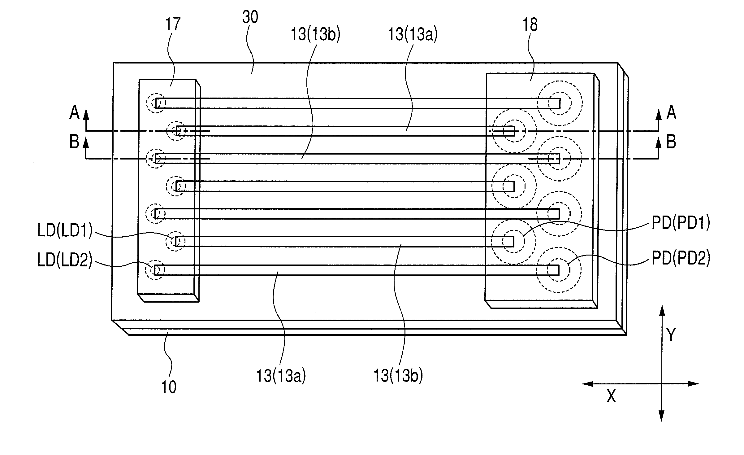
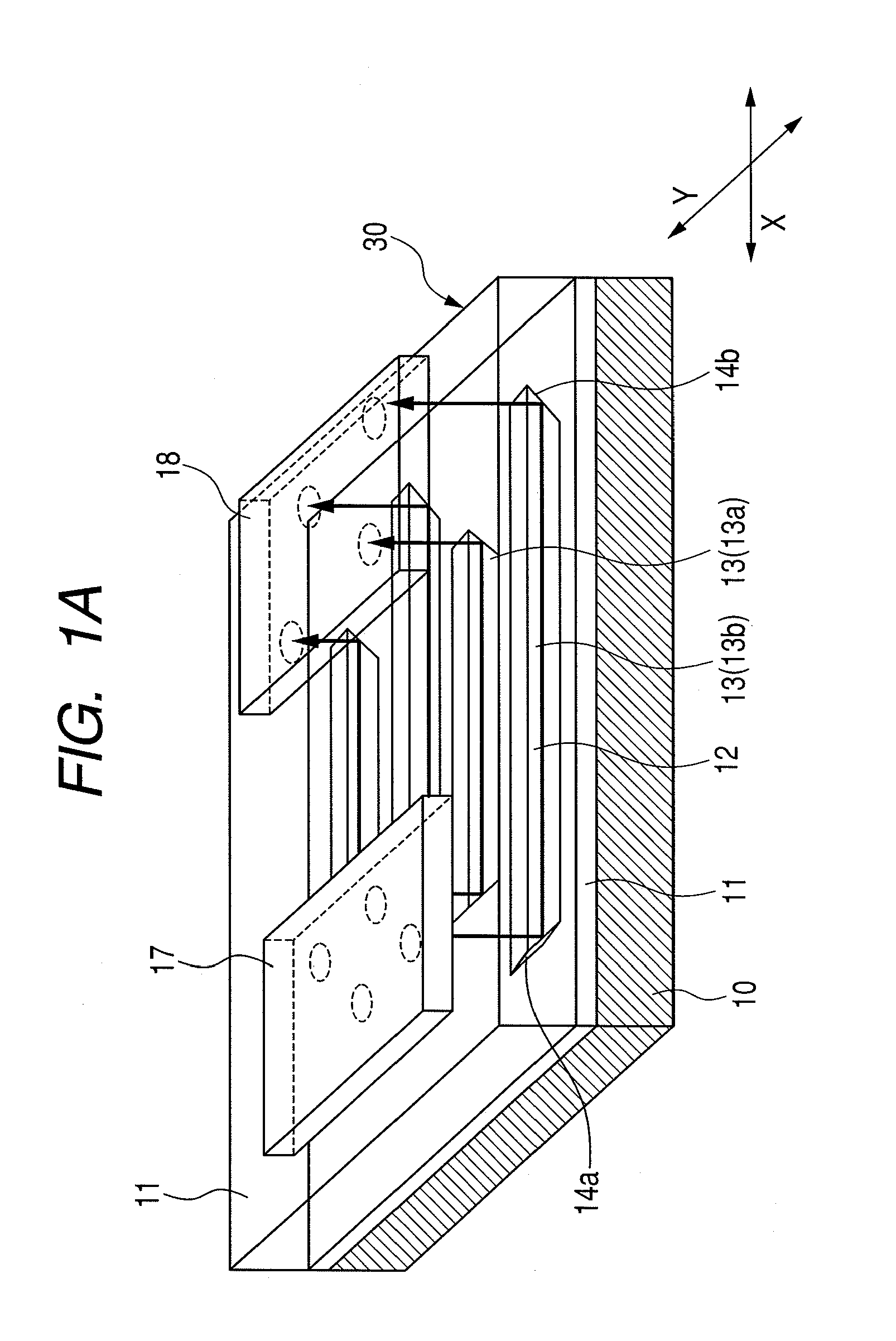
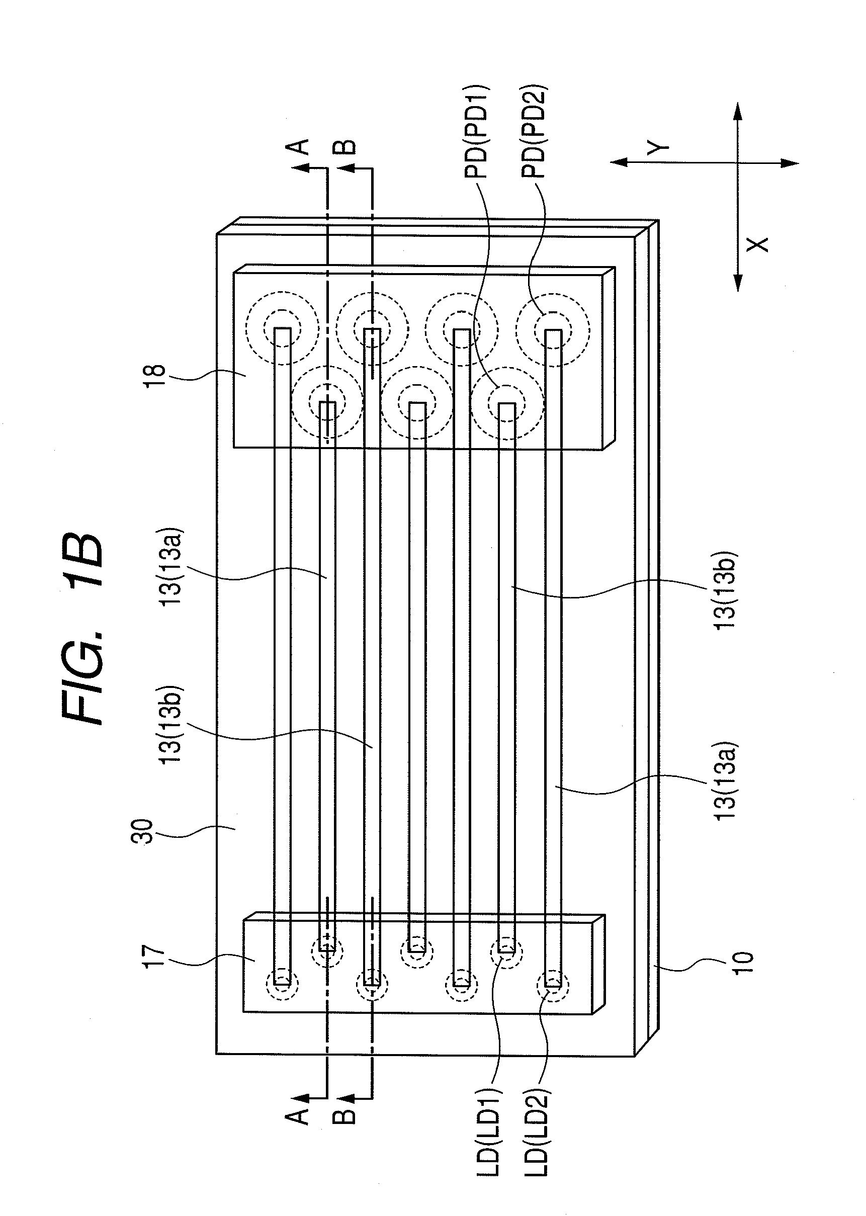
[0049]FIGS. 1A through 1D are drawings related to an optical interconnection assembled circuit in this first embodiment of the present invention.

[0050]FIG. 1A is a perspective view of the optical interconnection assembled circuit.

[0051]FIG. 1B is a flat (top) view of the optical interconnection assembled circuit.

[0052]FIG. 1C is a cross sectional view taken on line A-A of FIG. 1B.

[0053]FIG. 1D is a cross sectional view taken on line B-B of FIG. 1B.

[0054]As shown in FIGS. 1A through 1D, the optical interconnection assembled circuit in this first embodiment includes, for example, a laser diode array 17 and a photo diode array 18 assumed as optical element arrays, as well as an optical waveguide substrate 30 used for the optical connection between those optical element arrays (the laser diode array 17 and the photo diode array 18).

[0055]The optical waveguide substrate 30 includes a multi-channel optical waveguide array consisting of plural optical waveguides 13 on the same substrate. O...

second embodiment

[0095]FIG. 6 is a flat (top) view of an optical interconnection assembled circuit in this second embodiment of the present invention.

[0096]The optical interconnection assembled circuit in this second embodiment is basically the same in configuration with that in the first embodiment except for the following points.

[0097]In the first embodiment described above, as shown in FIGS. 1B through 1D, the optical waveguides 13a, as well as the optical waveguides 13b having a longer light path than that of the optical waveguides 13a respectively are disposed alternately and repetitively in the second direction (e.g., Y direction) and the laser diode LD1 in the first row (inside that in the second row) of the laser diode array 17 is connected optically to the photo diode PD1 in the first row (inside that in the second row) of the photo diode array 18 in the optical waveguide 13a of which light path is shorter than that of the optical waveguide 13b (inside—inside optical connection) while the l...

third embodiment

[0103]FIGS. 7A through 7C are drawings related to an optical interconnection assembled circuit in this third embodiment of the present invention.

[0104]FIG. 7A is a flat (top) view of the optical interconnection assembled circuit with respect to its schematic configuration.

[0105]FIG. 7B is a cross sectional view taken on line C-C of FIG. 7A.

[0106]FIG. 7C is a cross sectional view taken on line D-D of FIG. 7A.

[0107]The configuration of the optical interconnection assembled circuit in this third embodiment is basically the same as that in the first embodiment except for the following points.

[0108]In the first embodiment, the optical waveguide substrate 30 has a single layer optical waveguide array.

[0109]In this third embodiment, however, the optical waveguide substrate 30, as shown in FIGS. 7A through 7C, has a multilayer structure in which the optical waveguides 13a, as well as 13b that is longer than the optical waveguide 13a are formed in different layers. In this third embodiment, ...


PUM


Abstract

An optical interconnection assembled circuit capable of reducing the number of parts and components, as well as the number of manufacturing processes and capable of mounting those parts and components at a high density in an optical module, thereby realizing a low price. The optical interconnection assembled circuit includes a substrate including plural optical waveguides having partial tapered surfaces respectively, as well as an optical element array facing each of the tapered surfaces. In the optical interconnection assembled circuit, the tapered surfaces and the optical element array are fastened so that they face each other and the optical elements of the optical element array are staggered in disposition.

Description

CLAIM OF PRIORITY[0001]The present application claims priority from Japanese patent application JP 2009-038098 filed on Feb. 20, 2009, the content of which is hereby incorporated by reference into this application.FIELD OF THE INVENTION[0002]The present invention relates to an optical interconnection assembled circuit.BACKGROUND OF THE INVENTION[0003]Recently, in the field of information and telecommunications, optical communication traffics have been rapidly expanding to send / receive large capacity data. And so far, fiber-optic networks have been developed in order to meet the requirements of such optical communications in comparatively long distances of more than a few kilometers for backbone, metro, and access systems. In the near future, optical fibers will be used more and more for signal wirings to process large capacity data quickly even in extremely short distances of rack-to-rack (from a few meters to a few hundred meters) or of intra-rack (from a few centimeters to a few t...

Claims


Application Information

Patent Timeline
IPC IPC(8): G02B6/12G02B6/36
CPCG02B6/43G02B6/4214H01L2224/16225
Inventor MATSUOKA, YASUNOBUADACHI, KOICHIROSUGAWARA, TOSHIKI
Owner HITACHI LTD
Why Eureka
Try Eureka