Nonvolatile semiconductor memory device and manufacturing method for same

a semiconductor memory and non-volatile technology, applied in semiconductor devices, digital storage, instruments, etc., can solve the problems of difficult, or impossible, to detect the readout current, and achieve the effect of low cost, large capacity and low cos

Inactive Publication Date: 2010-09-02
SHARP KK
View PDF5 Cites 233 Cited by
  • Summary
  • Abstract
  • Description
  • Claims
  • Application Information

AI Technical Summary

Benefits of technology

[0030]The present invention can provide a nonvolatile semiconductor memory device with a three-dimensional memory cell array with a large capacity that can be fabricated at low cost. In particular, it becomes possible for RRAMs using 1R type or 1D1R type memory cells to have a multilayer structure, and the a memory cell array can be manufactured without increa...

Problems solved by technology

In recent years, however, the limit as to how far flash memories can be miniaturized has become evident, and nonvolatile memories, such as MRAMs (magnetoresistance variable memories), PCRAMs (phase variable memories), CBRAMs (solid electrolyte memories) and RRAMs (resistance variable memories), have been in development full steam.
However, 1R type memory cells do not have a current limiting element, and a parasitic current (leak current) flows through memory cells connected to unselected wires other than the memory cell formed between the two selected wires, and therefore, the parasitic current overlaps with the readout current that flows through the selected memory cell, and a problem arises, such that it becomes difficult, or impossible, to detect the readout current.
Though 1T1R type memory cells are excellent in terms of controllability because it is possible to control the strength and direction of the current that flows through the variable resistive elements, they occupy a large area and cannot easily provide a multilayer structure, and therefore, the memory capacity is largely limited by the c...

Method used


Image

  • Nonvolatile semiconductor memory device and manufacturing method for same
  • Nonvolatile semiconductor memory device and manufacturing method for same
  • Nonvolatile semiconductor memory device and manufacturing method for same

Examples


first embodiment

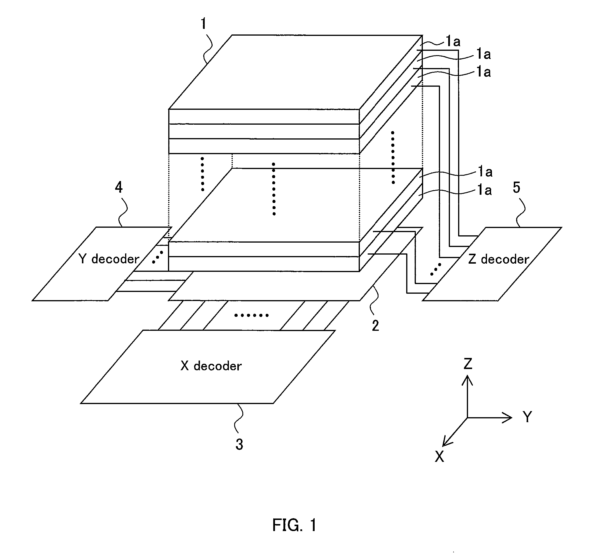
[0070]As schematically shown in FIG. 1, the device of the present invention is formed of a three-dimensional memory cell array 1, a two-dimensional array 2 of selection transistors, an X decoder 3, a Y decoder 4 and a Z decoder 5. The two-dimensional array 2, the X decoder 3 (corresponding to the first decoder), the Y decoder 4 (corresponding to the second decoder) and the Z decoder 5 (corresponding to the third decoder) are formed on the same substrate 6, and the three-dimensional memory cell array 1 is located above the two-dimensional array 2. Here, in the following description, the first direction and the second direction, which are parallel to the surface of the substrate 6 and perpendicular to each other, are the X direction and the Y direction, respectively, while the third direction, which is perpendicular to the surface of the substrate 6, is the Z direction.

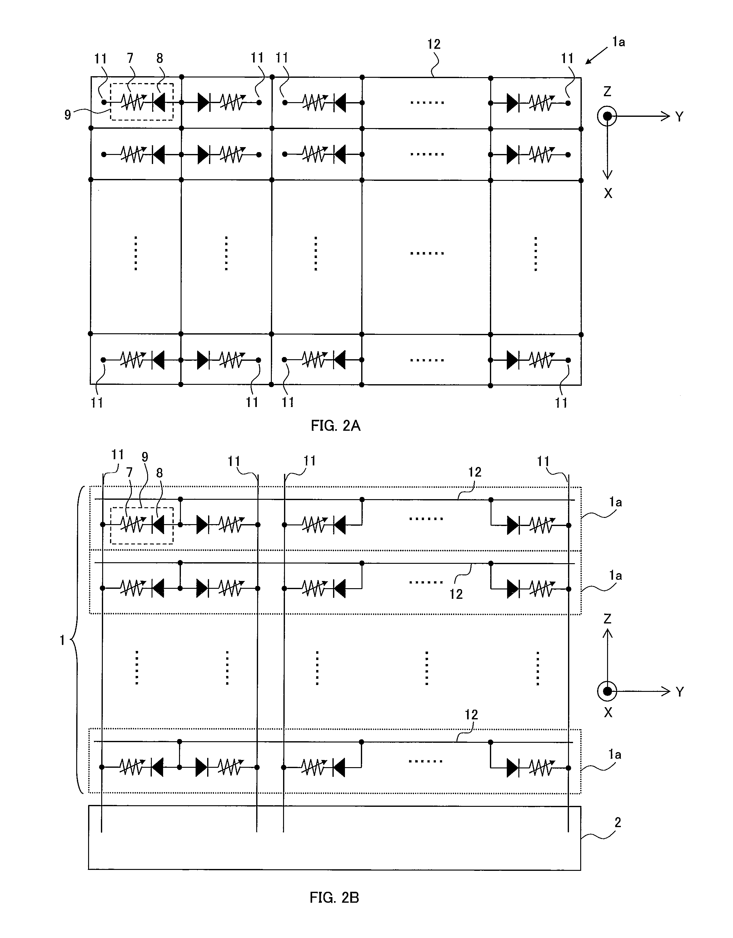
[0071]In the present embodiment, the three-dimensional memory cell array 1 is formed of a number of memory cells 9 wi...

second embodiment

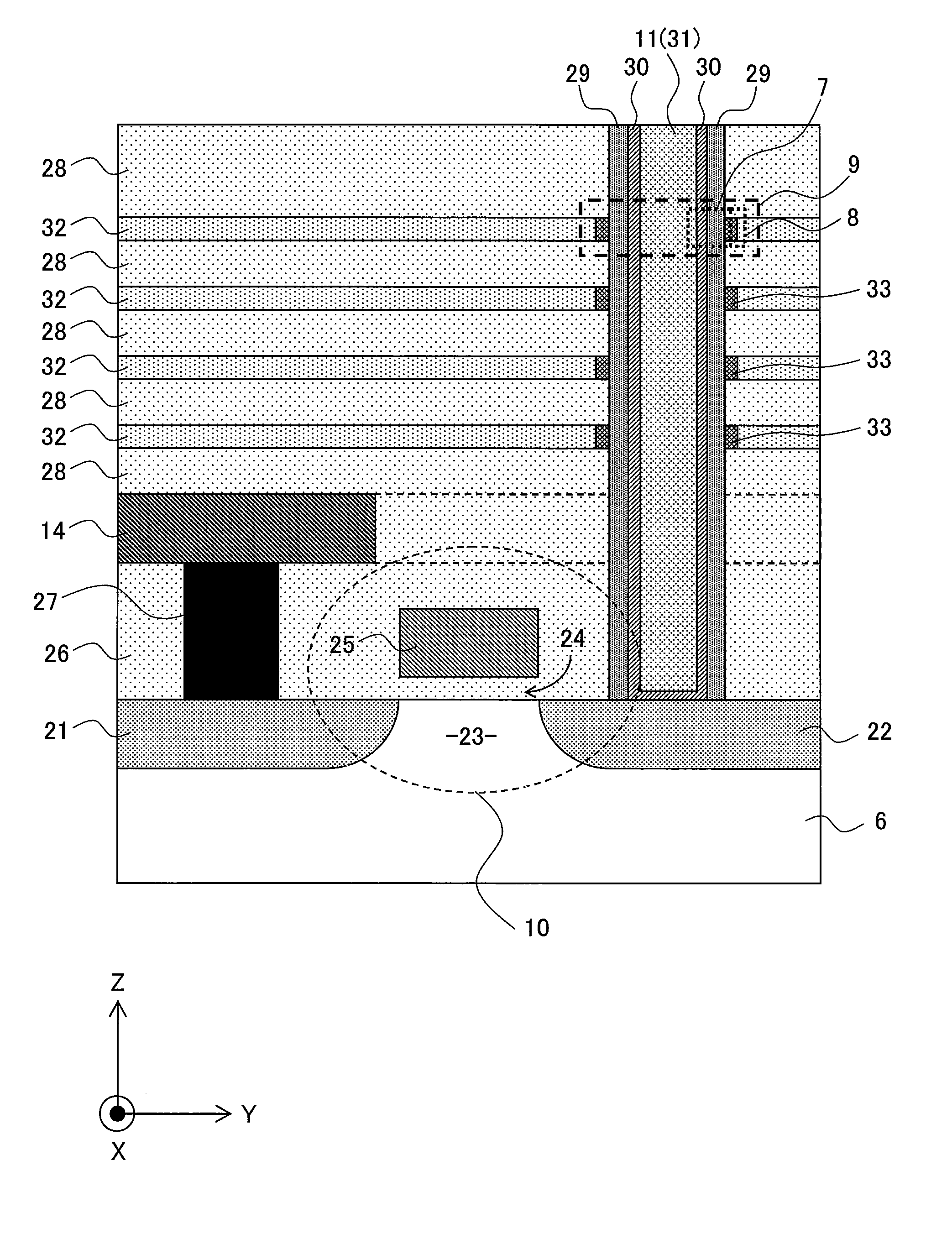
[0115]Next, the device according to the second embodiment of the present invention is described. According to the first embodiment shown in the above, selection transistors are formed of standard planar MOS transistors. In the case where selection transistors 10 are formed of planar MOS transistors in a two-dimensional array 2 having the wiring structure shown in FIG. 3, as shown in FIGS. 5 and 12, the electrodes for the drains 21, the sources 22 and the gates 25 are provided in a plane, and it is necessary to separate the contact holes 27 for connecting the drains 21 to the bit lines 14 and the through holes 34 for forming the middle selection lines 11 that are connected to the sources 22 from each other in the plane, and thus, a problem arises, such that the area occupied by each selection transistor 10, that is to say, the area occupied by each memory cell in the XY plane, is large in the three-dimensional memory cell array. When publicly known vertical MOS transistors are used a...

third embodiment

[0124]Next, the device according to the third embodiment of the present invention is described. Though 1D1R type memory cells are used as memory cells with two terminals in the above described first and second embodiments, the device of the present invention having the structure shown in FIG. 1 is possible even in the case where 1R type memory cells are used. This should be clear from the fact that the present invention does not relate to whether memory cells are of a 1R type or a 1D1R type, because the present invention is first characterized in that the three-dimensional memory cell array 1 and the two-dimensional array 2 of selection transistors 10 are combined via middle selection lines 11, so that the selection lines of the three-dimensional memory cell array 1 are formed only of the common plates 12 in an XY plane, and therefore, it is not necessary to use a photolithographic step using an expensive, state of the art stepper in order to form a two-dimensional memory cell array...


PUM


Abstract

A three-dimensional memory cell array of memory cells with two terminals having a variable resistive element is formed such that: one ends of memory cells adjacent in Z direction are connected to one of middle selection lines extending in Z direction aligned in X and Y directions; the other ends of the memory cells located at the same point in Z direction are connected to one of third selection lines aligned in Z direction; a two-dimensional array where selection transistors are aligned in X and Y directions is adjacent to the memory cell array in Z direction; gates of selection transistors adjacent in X direction, drains of selection transistors adjacent in Y direction and sources of selection transistors are connected to same first selection line, second selection line, and different middle selection lines, respectively; and first, second and third selection lines are connected to X, Y and Z decoders, respectively.

Description

CROSS REFERENCE TO RELATED APPLICATION[0001]This Nonprovisional application claims priority under 35 U.S.C. §119(a) on Patent Applications No. 2009-046221 filed in Japan on 27 Feb., 2009, No. 2009-115509 filed in Japan on 12 May, 2009, and No. 2009-241995 filed in Japan on 21 Oct., 2009 the entire contents of which are hereby incorporated by reference.BACKGROUND OF THE INVENTION[0002]1. Field of the Invention[0003]The present invention relates to a nonvolatile semiconductor memory device having a three-dimensional memory cell array where memory cells with two terminals having a nonvolatile variable resistive element are aligned in a three-dimensional matrix where the first direction, second and third direction are perpendicular to each other, as well as a manufacturing method for the same, and in particular, to a nonvolatile semiconductor memory device where the variable resistive element with two terminals that forms the memory cells reversibly changes between two or more different...

Claims


Application Information

Patent Timeline
IPC IPC(8): H01L45/00H01L21/822
CPCG11C13/0007H01L27/2454G11C2213/32G11C2213/34G11C2213/71G11C2213/72G11C2213/77H01L27/0688H01L27/101H01L45/08H01L45/1226H01L45/146H01L45/1616H01L27/2409H01L27/2418H01L27/2436H01L27/249G11C2013/0083H10B63/22H10B63/20H10B63/30H10B63/34H10B63/845H10N70/24H10N70/823H10N70/8833H10N70/023
Inventor AWAYA, NOBUYOSHIOHTA, YOSHIJITABUCHI, YOSHIAKI
Owner SHARP KK
Why Eureka
Try Eureka