Photovoltaic cell comprising an mis-type tunnel diode

Inactive Publication Date: 2010-09-09
GTAT CORPORATION
View PDF8 Cites 11 Cited by
  • Summary
  • Abstract
  • Description
  • Claims
  • Application Information

AI Technical Summary

Benefits of technology

[0005]A first aspect of the invention provides for a substantially crystalline semiconductor lamina having a first surface and a second surface opposite the first; a transparent conductive oxide; and an insulator layer having a thickness no more than about 40 angstroms, the insulator layer disposed between the lamina and the transparent conductive oxide, wherein the semiconductor lamina is lightly doped to a first conductivity type, the second surface of the lamina is nearer the insulator layer and the first surface of the lamina is farther from the insulator layer, and the first surface of the lamina is heavily doped to the first conductivity type, and wherein, during normal operation of the cell, charge carriers pass between the transparent conductive oxide and the lamina by tunneling through the insulator layer.
[0006]Another aspect of the invention provides for a photovoltaic cell comprising a substantially crystalline lamina having a light-facing surface and a back surface, the lamina having a thickness of about 50 microns or less; an insulator layer having a thickness no more than about 40 angstroms, the insulator layer disposed above the light-facing surface of the lamina; and a conductor disposed above the insulator layer and in immediate contact with the insulator layer.
[0007]Still another aspect of the invention provides for a photovoltaic cell comprising a substantially crystalline semiconductor lamina having a light-facing surface and a back surface, wherein th

Problems solved by technology

For some fabrication methods, however, high temperature s

Method used


Image

  • Photovoltaic cell comprising an mis-type tunnel diode
  • Photovoltaic cell comprising an mis-type tunnel diode
  • Photovoltaic cell comprising an mis-type tunnel diode

Examples


example

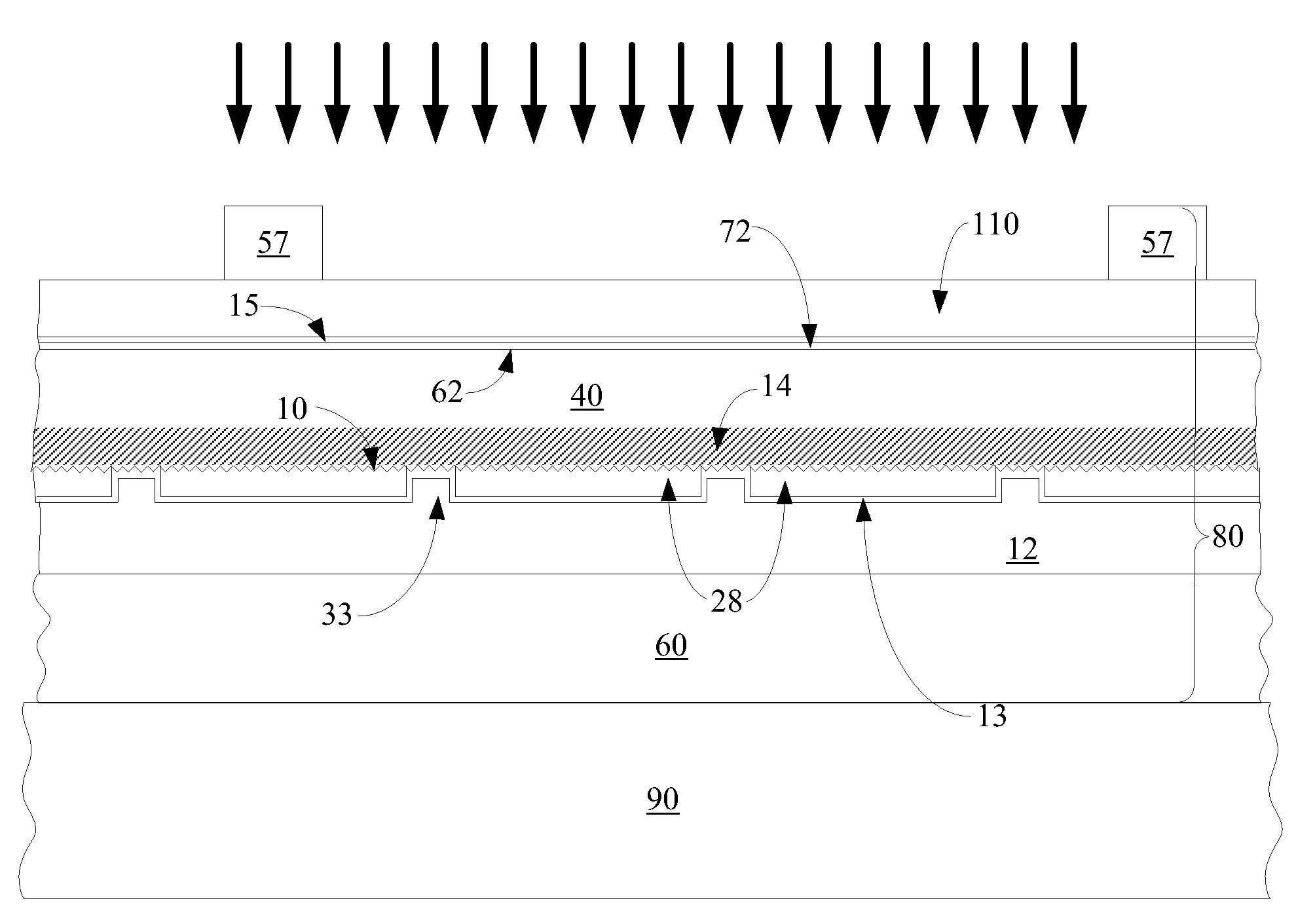
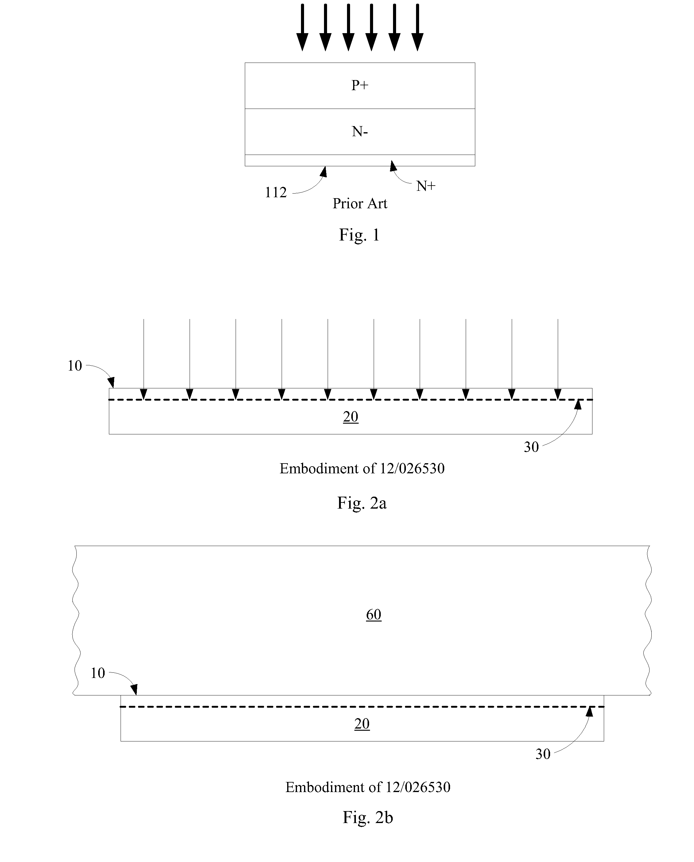
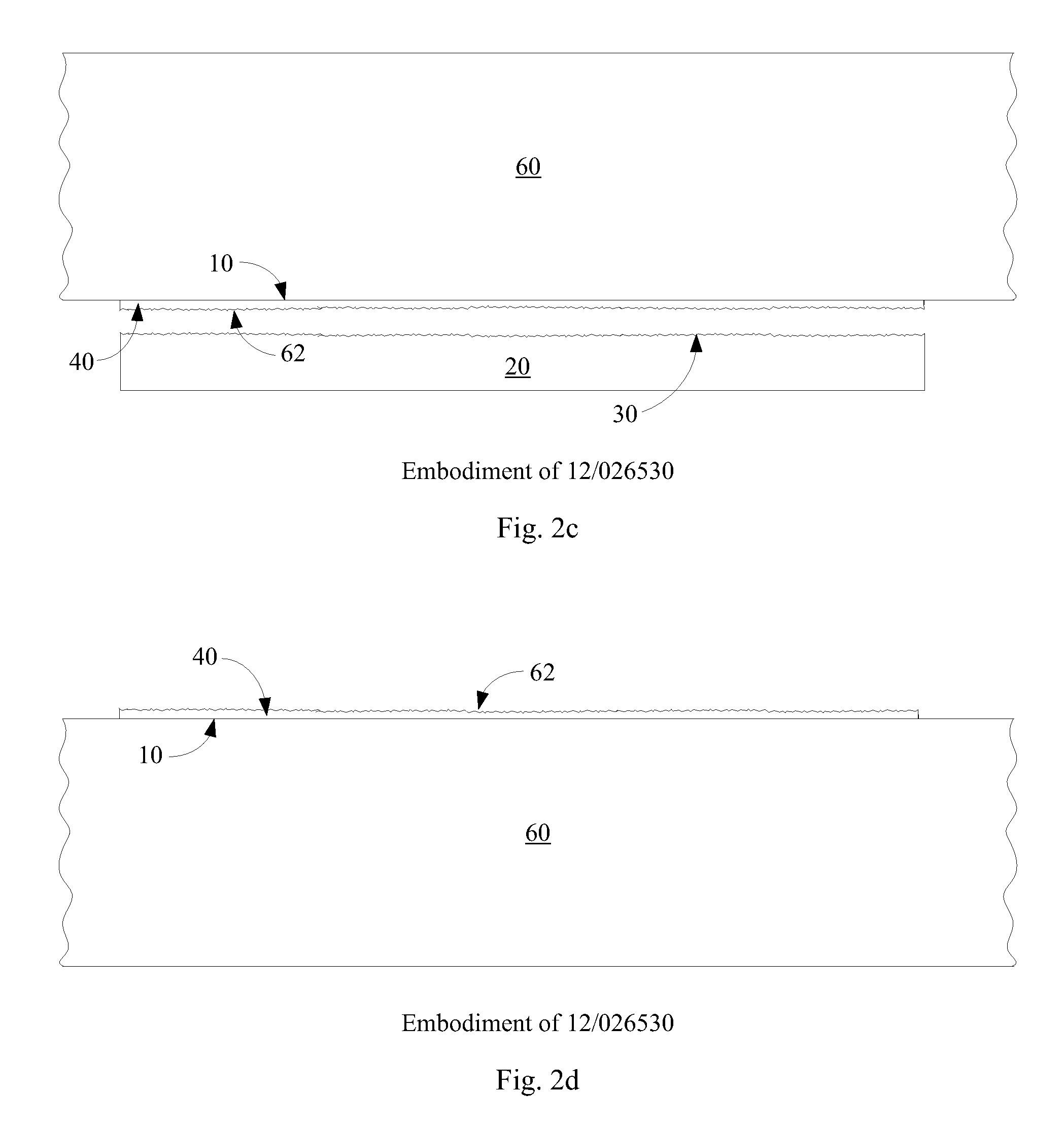
MIS-Type Tunnel Diode with TCO

[0032]The process begins with a donor body of an appropriate semiconductor material. An appropriate donor body may be a monocrystalline silicon wafer of any practical thickness, for example from about 200 to about 1000 microns thick. In alternative embodiments, the donor wafer may be thicker; maximum thickness is limited only by practicalities of wafer handling. Alternatively, polycrystalline or multicrystalline silicon may be used, as may microcrystalline silicon, or wafers or ingots of other semiconductors materials, including germanium, silicon germanium, or III-V or II-VI semiconductor compounds such as GaAs, InP, etc. In this context the term multicrystalline typically refers to semiconductor material having grains that are on the order of a millimeter or larger in size, while polycrystalline semiconductor material has smaller grains, on the order of a thousand angstroms. The grains of microcrystalline semiconductor material are very small, for exa...


PUM


Abstract

A photovoltaic cell comprising a thin semiconductor lamina is described; the lamina is formed by cleaving from a donor wafer while the wafer is bonded to a receiver element which provides mechanical support. Thus fabrication steps performed following cleaving are advantageously performed at temperatures that will not damage the receiver element. By fabricating a cell comprising an MIS-type tunnel diode, rather than a conventional p-n diode, a high-temperature doping step may be avoided.

Description

BACKGROUND OF THE INVENTION[0001]The invention relates to a photovoltaic cell including an MIS-type tunnel diode.[0002]In a photovoltaic cell, incident photons create free charge carriers. An electric field directs these free carriers into current. The electric field most often results from a p-n diode within the photovoltaic cell. A cell including a p-n diode is most economically formed by doping opposing faces of the cell with, respectively, p-type and n-type dopants. The conventional methods of performing these doping steps are performed at high temperature. For some fabrication methods, however, high temperature steps at some point in the process may be disadvantageous.[0003]There is a need, therefore, for a photovoltaic cell that does not operate as a p-n diode which can be fabricated at a lower temperature.SUMMARY OF THE PREFERRED EMBODIMENTS[0004]The present invention is defined by the following claims, and nothing in this section should be taken as a limitation on those clai...

Claims


Application Information

Patent Timeline
IPC IPC(8): H01L31/00H01L21/70
CPCY02E10/50H01L31/062
Inventor HILALI, MOHAMMED M.PETTI, CHRISTOPHER J.
Owner GTAT CORPORATION
Why Eureka
Try Eureka