Leakage Reduction in Memory Devices

Inactive Publication Date: 2010-09-09
QUALCOMM INC
View PDF5 Cites 5 Cited by
  • Summary
  • Abstract
  • Description
  • Claims
  • Application Information

AI Technical Summary

Benefits of technology

[0010]According to one aspect of the disclosure, a memory device includes a core array including a plurality of memory cells and

Problems solved by technology

The thickness of the insulator is small enough, however, that some current passes or “leaks” through the transistor even when turned “off”.
The leakage current results in unnecessary power consumption.
Although power consumption attributed to leakage current is small for an individual transistor, when multiplied over the millions of transistors that may be present in a memory device, the cumulative resultant power consumption attributed to leakage current is significant.
Therefore, a reduction in thickness of the transistor corresponds to larger leakage currents.
This increase in leakage current results in larger power consumption by the memory device.
High threshold transistors, on the other hand, have significantly reduced leakage current when turned “off” but suffer from poor performance.
Use of high threshold transistors has, however, been limite

Method used


Image

  • Leakage Reduction in Memory Devices
  • Leakage Reduction in Memory Devices
  • Leakage Reduction in Memory Devices

Examples


Embodiment Construction

[0022]The present disclosure will be explained and better understood by reference to exemplary systems in which the disclosed circuitry may be employed, conventional devices used in such a system, and a detailed discussion of devices that may be used in such a system to provide reduced power consumption.

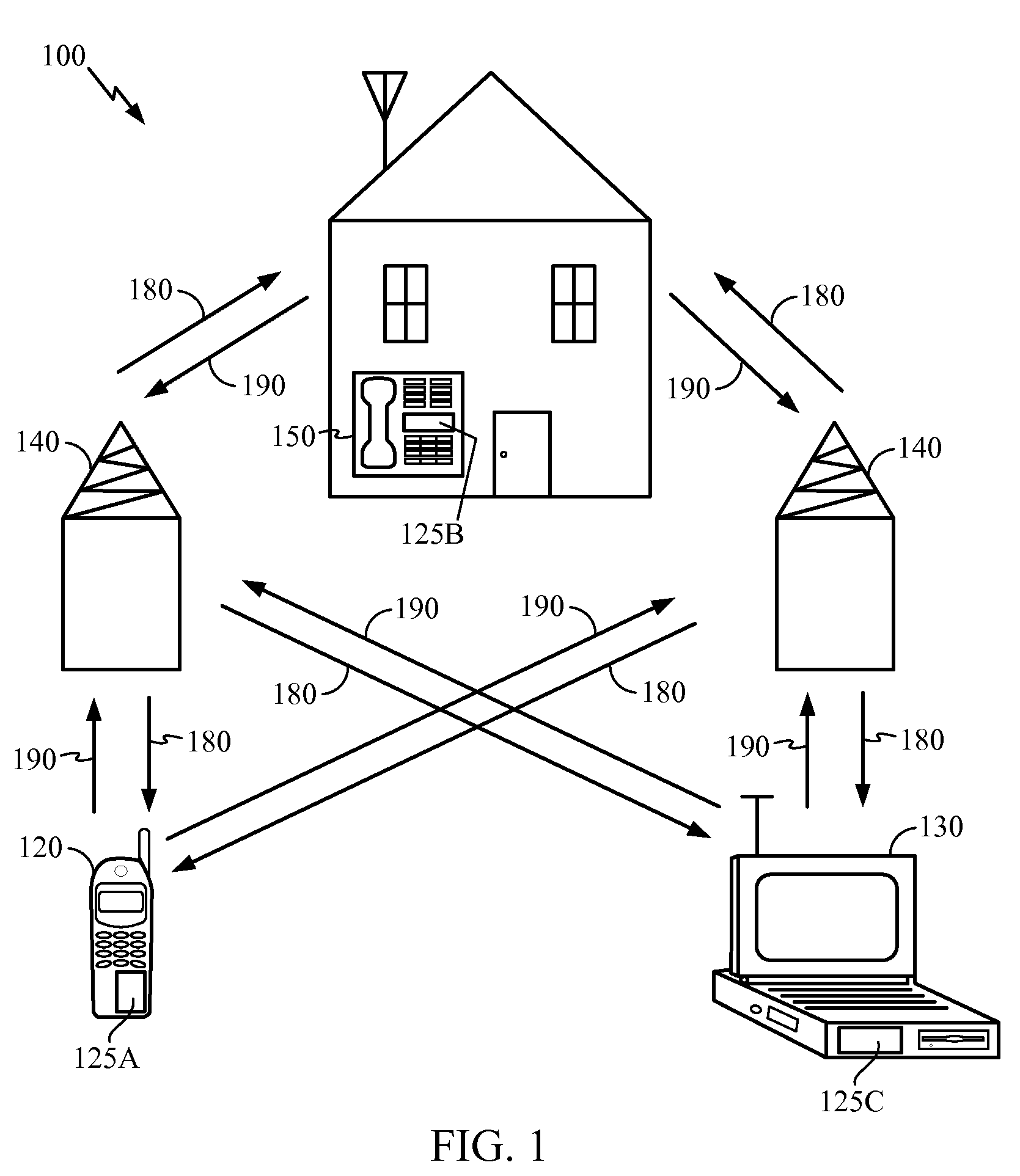
[0023]FIG. 1 shows an exemplary wireless communication system 100 in which an embodiment of the disclosure may be advantageously employed. For purposes of illustration, FIG. 1 shows three remote units 120, 130, and 150 and two base stations 140. It will be recognized that typical wireless communication systems may have many more remote units and base stations. The remote units 120, 130, and 150 include IC devices 125A, 125B and 125C, that include the disclosed memory device. It will be recognized that any device containing an IC may also include the disclosed memory device, including the base units. FIG. 1 shows forward link signals 180 from the base stations 140 and the remote units...


PUM


Abstract

A memory device includes a core array that includes memory cells. The memory device also includes a headswitch coupled to the core array and a positive supply voltage. The headswitch reduces leakage current from the core array by disconnecting the core array from the positive supply voltage. Additionally, head switches are added for pre-charge devices to further reduce leakage current.

Description

TECHNICAL FIELD[0001]This disclosure relates to integrated circuits (ICs). More specifically, it relates to memory devices and, even more specifically, to reducing power consumption of memory devices.BACKGROUND[0002]A memory device or memory can generally be described as hardware that can store data for later retrieval. Memory devices generally include a set of transistors used to store data (represented, for example, by an electrical charge) and a set of transistors used to control access to the data store. Individual transistors generally include a very thin insulating layer that separates a metal layer from a semiconductor layer. The insulator stops current flow when the transistor is switched “off”.[0003]Ideally in the “off” scenario no current passes through the transistor and no power is consumed. The thickness of the insulator is small enough, however, that some current passes or “leaks” through the transistor even when turned “off”. The leakage current results in unnecessary...

Claims


Application Information

Patent Timeline
IPC IPC(8): G11C7/00G11C5/14
CPCG11C7/22G11C8/08G11C11/4094G11C7/00G11C2207/2227H03K19/0016G11C11/413
Inventor JUNG, CHANGHOCHEN, NANZHONG, CHENGCHEN, ZHIQIN
Owner QUALCOMM INC
Why Eureka
Try Eureka