

Circuit device
- Summary
- Abstract
- Description
- Claims
- Application Information
AI Technical Summary
Benefits of technology
Problems solved by technology
Method used
Image

Examples
embodiment 1
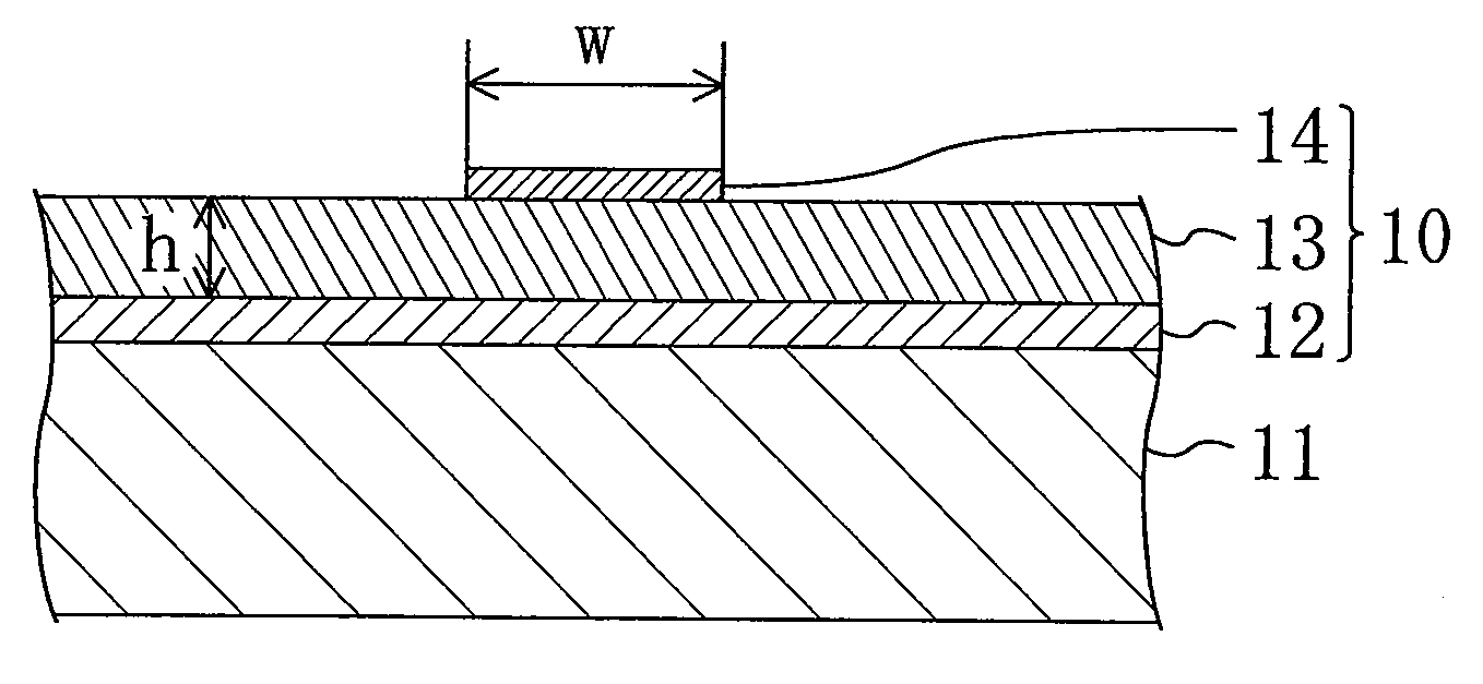
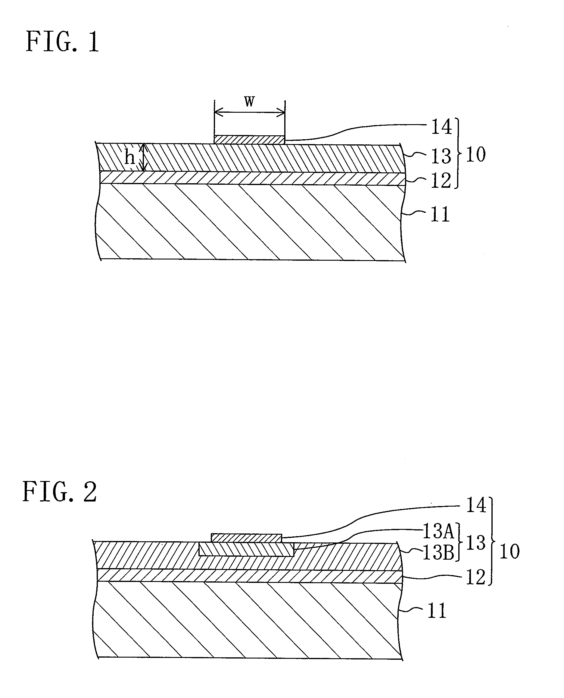
[0066]Embodiment 1 of the present invention will be described with reference to the drawings. FIG. 1 illustrates a cross-sectional configuration of a circuit device according to Embodiment 1. As shown in FIG. 1, the circuit device of the present embodiment includes a ground conductor 12 formed on a substrate 11, a dielectric film 13 made of a nano-composite film formed on the ground conductor 12, and a signal line 14 formed on the dielectric film 13. The ground conductor 12, the dielectric film 13, and the signal line 14 constitute a transmission line 10 serving as a microstrip line. The impedance of the microstrip line is determined according to mainly the width w of the signal line 14, the thickness h of the dielectric film 13, and the relative dielectric constant of the dielectric film 13. For this reason, when the dielectric film 13 is made of a benzocyclobutene (BCB) film having a relative dielectric constant of 2.65, the ratio between the width w and the thickness h needs to b...
embodiment 2
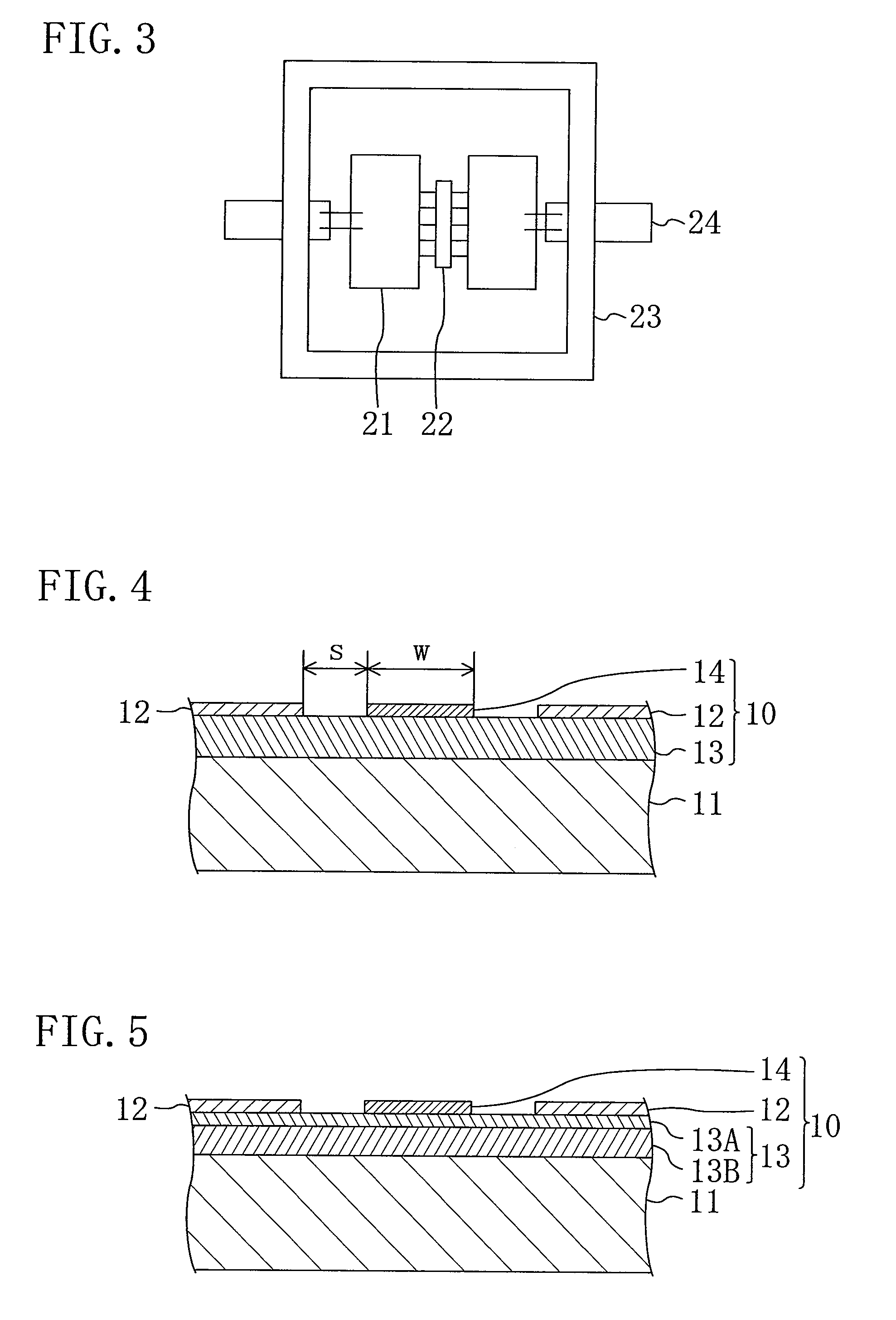
[0076]Embodiment 2 of the present invention will be described below with reference to the drawings. FIG. 4 illustrates a cross-sectional configuration of a circuit device according to Embodiment 2. In FIG. 4, the same reference symbols as those shown in FIG. 1 are used to represent equivalent elements, and the explanation thereof will be omitted.
[0077]As shown in FIG. 4, as a transmission line 10, the circuit device of the present embodiment includes a coplanar line instead of the microstrip line. For this reason, on a dielectric film 13, a signal line 14 and ground conductors 12 are formed. The signal line 14 is formed between the two ground conductors 12, and the signal line 14 extends parallel to the ground conductors 12.
[0078]The impedance of the coplanar line is determined according to the ratio between the signal line width w and the gap s between the signal line 14 and the ground conductor 12. Therefore, in order to increase the line width w, the gap s needs to be enlarged. H...
embodiment 3
[0085]Embodiment 3 of the present invention will be described below with reference to the drawings. FIG. 8 illustrates a cross-sectional configuration of a circuit device according to Embodiment 3. In FIG. 8, the same reference symbols as those shown in FIG. 1 are used to represent equivalent elements, and the explanation thereof will be omitted.
[0086]As shown in FIG. 8, a circuit device of the present embodiment includes a metal-insulator-metal (MIM) capacitor 30 formed on an insulator 34 on a substrate 11. The MIM capacitor 30 includes a nano-composite film 33 formed over the substrate 11, and a lower electrode 31 and an upper electrode 32 facing each other with the nano-composite film 33 provided therebetween.
[0087]Circuit devices such as MMICs often require a capacitor. When a nano-composite film having a high relative dielectric constant is used as a capacitative insulator of the capacitor as in the present embodiment, it is possible to achieve a high capacitance value even wit...
PUM
 Abstract
Description
Claims
Application Information