Semiconductor laser structure

Inactive Publication Date: 2010-09-23
DENSO CORP
View PDF6 Cites 3 Cited by
  • Summary
  • Abstract
  • Description
  • Claims
  • Application Information

AI Technical Summary

Benefits of technology

[0011]In view of the above-described problem, it is an object of the present disclosure to provide a semiconductor laser structure with a low resistance and high crystallinity.
[0013]Since the dopants in the P conductive type layer and the N conductive type layer are restricted from being diffused into other layers, high concentration of the dopants in the P conductive type layer and the N conductive type layer is maintained. As a result, resistance in the semiconductor laser structure with using the tunnel junction layer is reduced. Further, since the P conductive type dopant does not provide etching function after decomposition, crystallinity is not reduced. Further, a manufacturing method of the laser structure is simple.

Problems solved by technology

Further, since the P conductive type dopant does not provide etching function after decomposition, crystallinity is not reduced.

Method used


Image

  • Semiconductor laser structure
  • Semiconductor laser structure
  • Semiconductor laser structure

Examples


first example embodiment

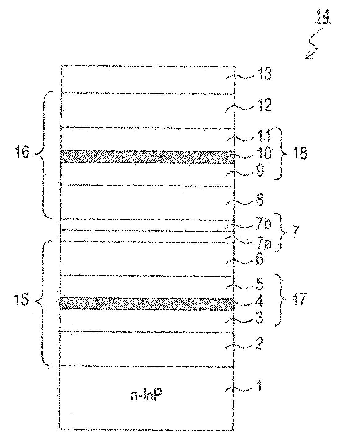
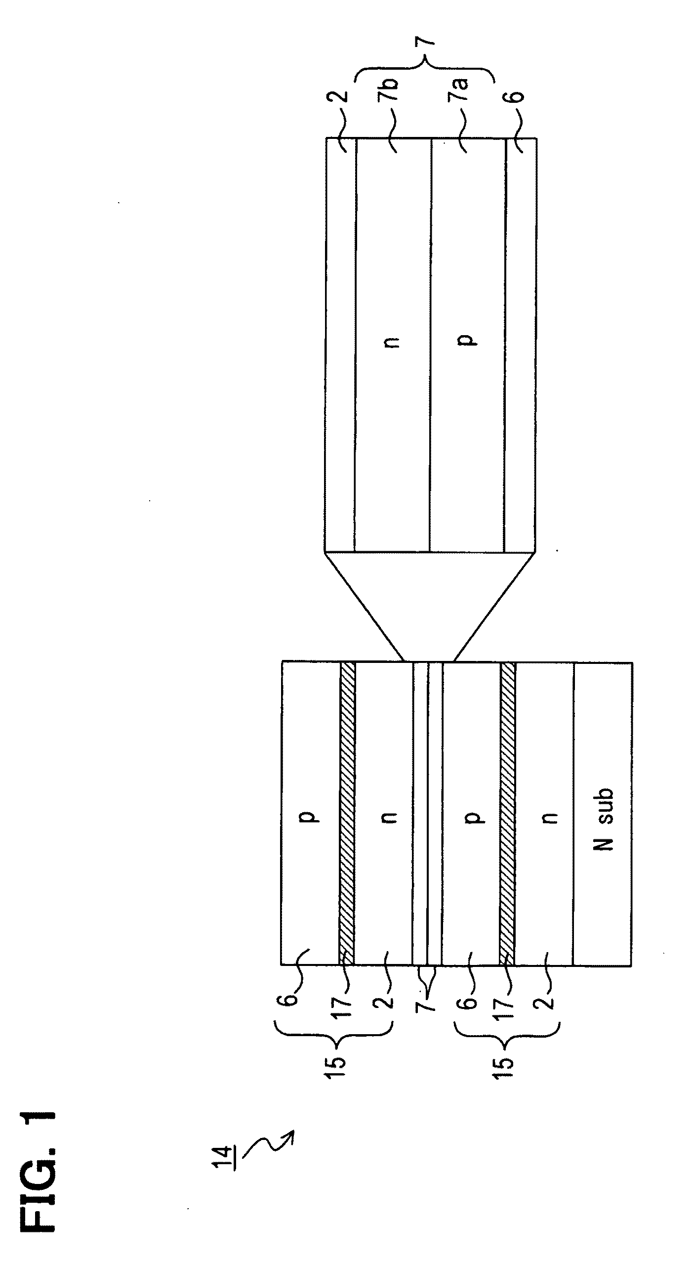
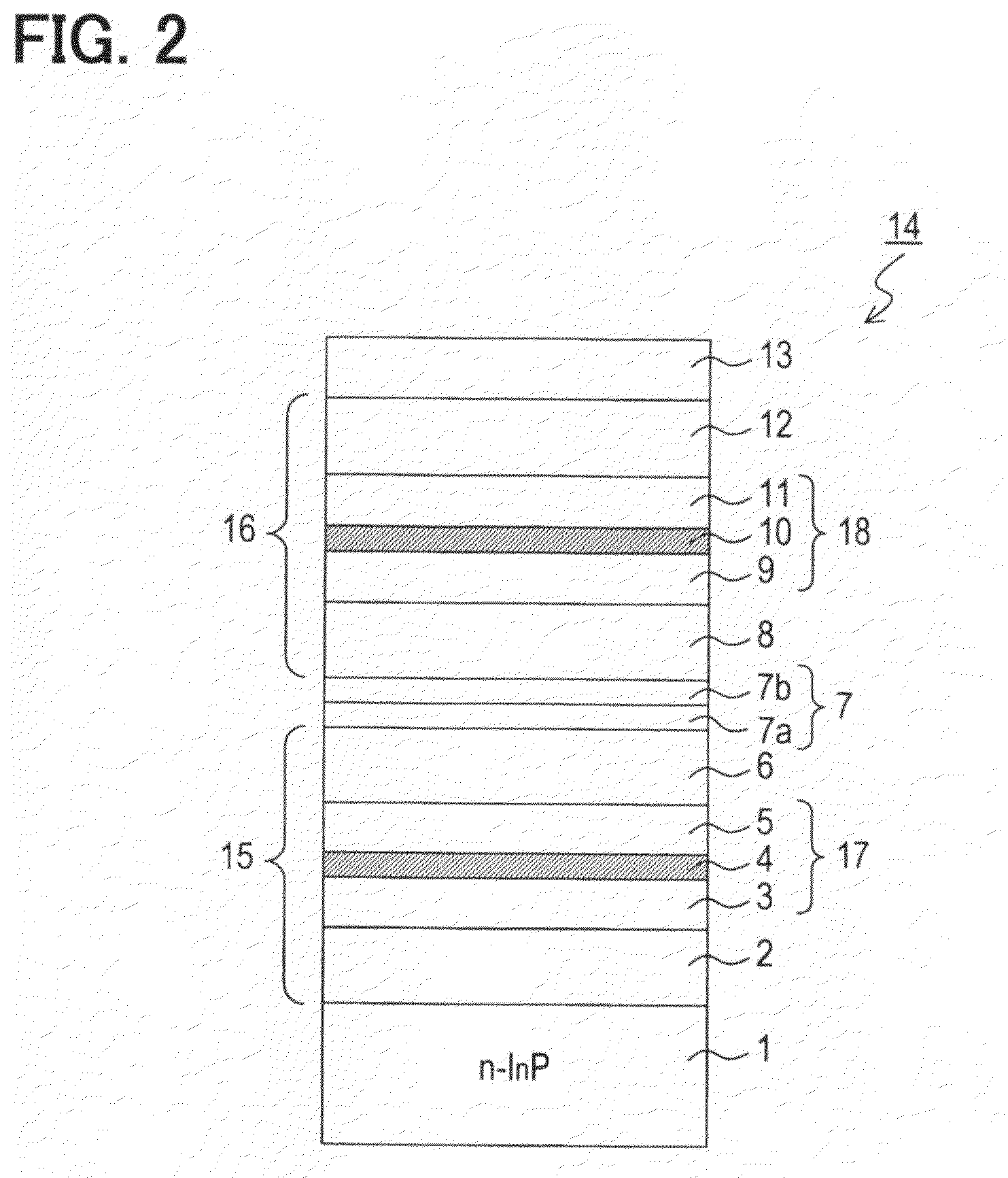
[0038]FIG. 2 shows a laser structure 14 according to a first example embodiment. The structure 14 includes a substrate 1 made of N conductive type InP, a N conductive type clad layer 2, a N conductive type waveguide layer 3, a multiple quantum well active layer 4, a P conductive type waveguide layer 5, a P conductive type clad layer 6, a P conductive type layer 7a, a N conductive type layer 7b, a N conductive type clad layer 8, a N conductive type waveguide layer 9, a multiple quantum well active layer 10, a P conductive type waveguide layer 11, a P conductive type clad layer 12, and a P conductive, type contact layer 13, which are stacked in this order. Each layer is formed by a conventional MOCVD method. A substrate temperature in a growth process is in a range between 550° C. and 800° C.

[0039]A composition, a thickness, a carrier concentration and a dopant in each layer are shown in FIG. 9.

[0040]The N conductive type clad layer 2, the N conductive type waveguide layer 3, the mult...

second example embodiment

[0049]FIG. 6 shows a laser structure 14 according to a second example embodiment. The structure 14 includes a substrate 1 made of N conductive type GaAs, a N conductive type clad layer 2, a N conductive type waveguide layer 3, a multiple quantum well active layer 4, a P conductive type waveguide layer 5, a P conductive type clad layer 6, a P conductive type layer 7a, a N conductive type layer 7b, a N conductive type clad layer 8, a N conductive type waveguide layer 9, a multiple quantum well active layer 10, a P conductive type waveguide layer 11, a P conductive type clad layer 12, and a P conductive type contact layer 13, which are stacked in this order. Each layer is formed by a conventional MOCVD method. A substrate temperature in a growth process is in a range between 550° C. and 800° C.

[0050]A composition, a thickness, a carrier concentration and a dopant in each layer are shown in FIG. 10.

[0051]The N conductive type clad layer 2, the N conductive type waveguide layer 3, the mu...


PUM


Abstract

A semiconductor laser structure includes: a plurality of laser structure units, wherein each laser structure unit includes a N conductive type clad layer, a light emission layer and a P conductive type clad layer, which are stacked in this order; and a tunnel junction layer disposed between two adjacent laser structure units. The tunnel junction layer includes a P conductive type layer and a N conductive type layer. The P conductive type layer includes a dopant of zinc. The N conductive type layer includes a dopant of a group six element.

Description

CROSS REFERENCE TO RELATED APPLICATION[0001]This application is based on Japanese Patent Application No. 2009-68510 filed on Mar. 19, 2009, the disclosure of which is incorporated herein by reference.FIELD OF THE INVENTION[0002]The present invention relates to a semiconductor laser structure.BACKGROUND OF THE INVENTION[0003]When a semiconductor laser device is used for an apparatus such as a laser radar apparatus for generating a high power according to a large pulse current, as shown in FIG. 7, multiple laser structure units 101, 103 are stacked on a growing surface of a substrate 105 in a vertical direction of the substrate 105. A first laser structure unit 101 includes a N conductive type clad layer 107, a light emission layer 109 and a P conductive type clad layer 111, which are stacked in this order. A second laser structure unit 103 includes a N conductive type clad layer 113, a light emission layer 115 and a P conductive type clad layer 117, which are stacked in this order.[0...

Claims


Application Information

Patent Timeline
IPC IPC(8): H01S5/34H01S5/026H01S5/323
CPCB82Y20/00H01S5/0425H01S5/305H01S2304/04H01S5/34313H01S5/4018H01S5/4031H01S5/3095H01S5/04252
Inventor MATSUSHITA, NORIYUKIYAMADA, HITOSHI
Owner DENSO CORP
Why Eureka
Try Eureka