This helps you quickly interpret patents by identifying the three key elements:
Problems solved by technology
Method used
Benefits of technology
Benefits of technology
[0024]Accordingly, the present invention has been accomplished in view of the above problems, and it is, therefore, an object of the present invention to provide a thin film transistor which suppresses the occurrence of a hump in the transfer characteristics of the thin film transistor in which an oxide semiconductor is used for a semiconductor layer, and a method of producing the same.
[0034]According to the present invention, occurrence of a hump in the transfer characteristics of a thin film transistor in which an oxide semiconductor is used for a semiconductor layer can be suppressed.
[0035]Further, according to the present invention, a thin film transistor which can suppress occurrence of a hump in the transfer characteristics of the thin film transistor in which an oxide semiconductor is used for a semiconductor layer can be produced.
Problems solved by technology
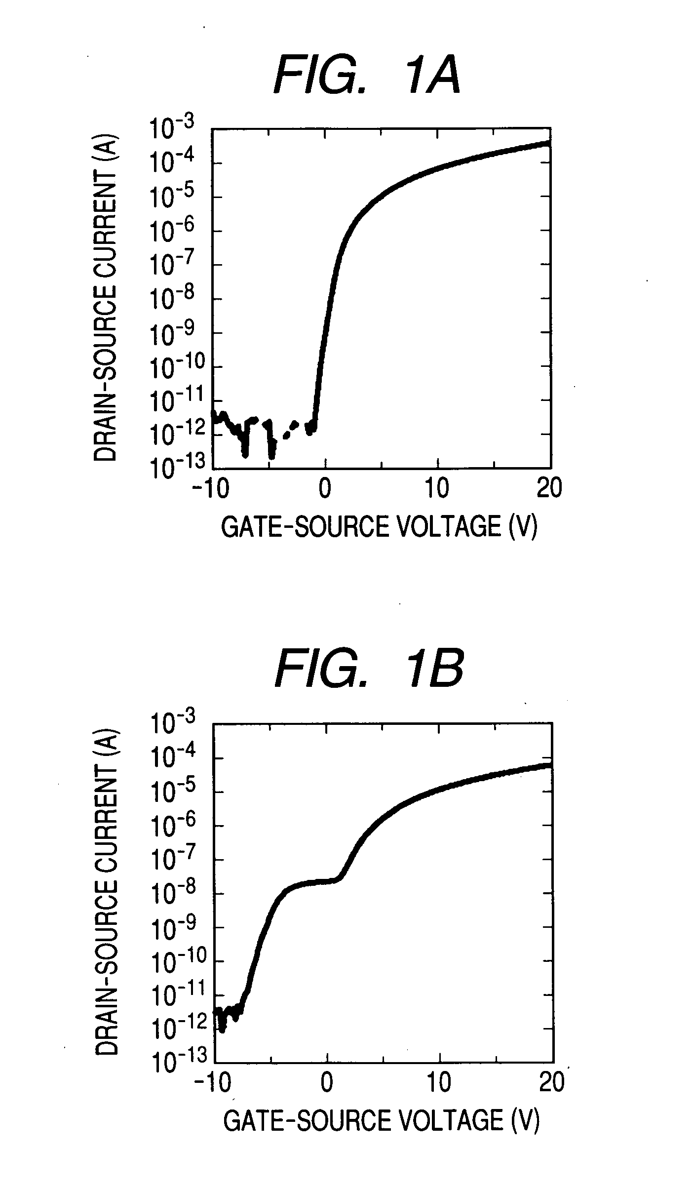
One problem which arises when a thin film transistor is produced and used is the so-called “hump” which appears in drain current (Ids)—gate voltage (Vgs) characteristics (transfer characteristics). FIG. 1B illustrates typical transfer characteristics of a thin film transistor in which a hump is observed.
Therefore, if a hump is formed, a malfunction occurs in which a desired emission intensity cannot be obtained.
However, in the case of the above-mentioned thin film transistor in which an oxide semiconductor is used for a semiconductor layer, the mechanism of operation of the transistor is different from that of a polysilicon thin film transistor.
However, particularly in a bottom gate thin film transistor, because there is only the protective layer on the semiconductor layer, if the protective layer does not function sufficiently, the back gate interface may be modified to cause a hump in the transfer characteristics.
Method used
Image
Click on the blue label to locate the original text in one second.
Reading with bidirectional positioning of images and text.
Examples
example 1
[0102]FIG. 7 is a cross-sectional view illustrating the configuration of a thin film transistor according to Example 1 of the present invention. As illustrated in FIG. 7, this example is a bottom-contact type double-gate thin film transistor. The thin film transistor illustrated in FIG. 7 is formed on a substrate 1.
[0103]More specifically, a first gate electrode 2, a first gate insulating layer 3, a drain electrode 5, a source electrode 6, a semiconductor layer 4, a second gate insulating layer 7, and a second gate electrode 8 are formed on the substrate 1.
[0104]A glass substrate (No. 1737 manufactured by Corning Incorporated) is used as the substrate 1. The thickness of the glass substrate is 0.5 mm.
[0105]A Mo thin film is formed on the substrate 1 in the thickness of 50 nm. In this example, DC magnetron sputtering using an atmosphere of an argon gas is used to form the MO thin film.
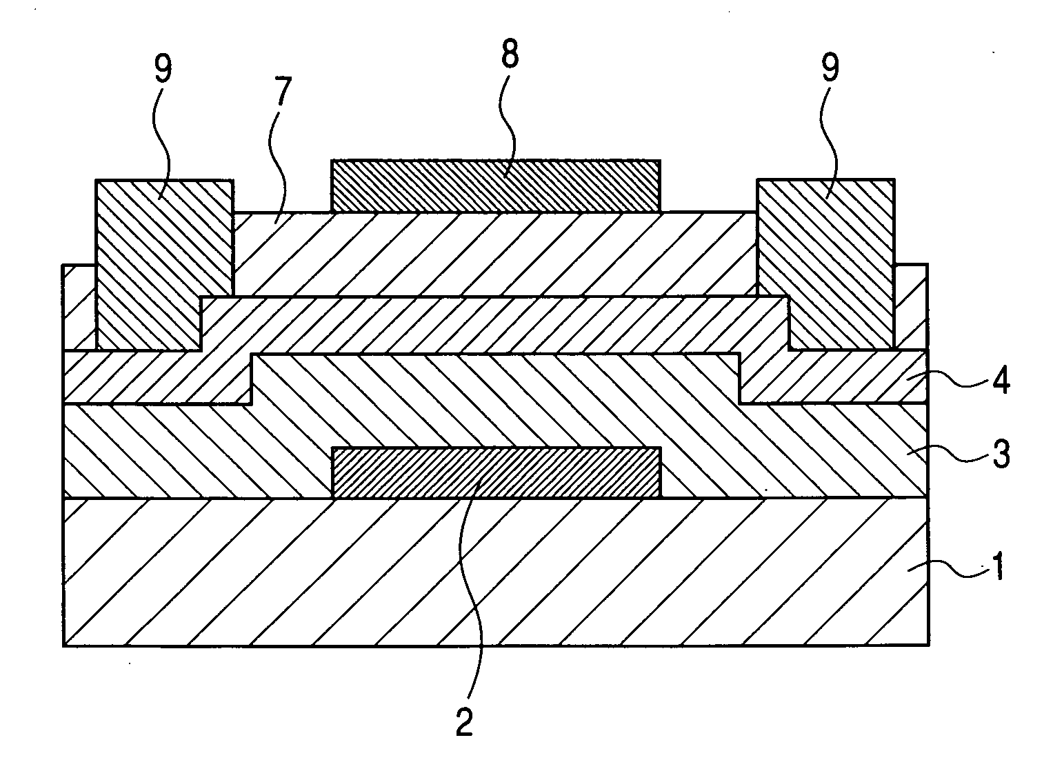
[0127]FIG. 10 is a cross-sectional view illustrating the configuration of a thin film transistor according to Example 2 of the present invention. This example is an example of forming a planar double-gate thin film transistor. The thin film transistor illustrated in FIG. 10 is formed on a substrate 1.
[0128]More specifically, on the substrate 1, there are formed a first gate electrode 2, a first gate insulating layer 3, a semiconductor layer 4, a drain electrode 5, a source electrode 6, a second gate insulating layer 7, a second gate electrode 8, contact electrodes 9, and a protective layer 10.
[0129]A glass substrate (No. 1737 produced by Corning Incorporated) is used as the substrate 1. The thickness of the glass substrate is 0.5 mm.
[0130]First, a Mo thin film is formed on the substrate 1 in a thickness of 50 nm. In this example, DC magnetron sputtering using an atmosphere of argon gas is used to form the Mo thin film.
[0131]Then, the deposited Mo thin film is finely processed by pho...
PUM
Abstract
A first gate electrode (2) is formed on a substrate (1); a first gate insulating layer (3) is formed so as to cover the first gate electrode (2); a semiconductor layer (4) including an oxidesemiconductor is formed on the first gate insulating layer (3); a second gate insulating layer (7) is formed on the semiconductor layer (4); a second gate electrode (8) having a thickness equal to or larger than a thickness of the first gate electrode (2) is formed on the second gate insulating layer (7); and a drain electrode (6) and a source electrode (5) are formed so as to be connected to the semiconductor layer (4).
Description
TECHNICAL FIELD[0001]The present invention relates to a thin film transistor and a method of producing the same. More particularly, the present invention relates to a double-gate thin film transistor and a method of producing the same.BACKGROUND ART[0002]A thin film transistor is a kind of a field-effect transistor and is mainly applied to an active matrixliquid crystal display and an active matrix organic EL display.[0003]At present the mainstream of the thin film transistor is a polysilicon thin film transistor in which polycrystalline silicon is used for a semiconductor layer and an amorphous silicon thin film transistor in which amorphous silicon is used for a semiconductor layer.[0004]With regard to the polysilicon thin film transistor in which the mobility of electrons is several hundred times greater than that of the amorphous silicon thin film transistor, not only a technology for a type formed at high temperatures but also a technology for a type formed at low temperatures...
Claims
Application Information
Patent Timeline
Application Date:The date an application was filed.
Publication Date:The date a patent or application was officially published.
First Publication Date:The earliest publication date of a patent with the same application number.
Issue Date:Publication date of the patent grant document.
PCT Entry Date:The Entry date of PCT National Phase.
Estimated Expiry Date:The statutory expiry date of a patent right according to the Patent Law, and it is the longest term of protection that the patent right can achieve without the termination of the patent right due to other reasons(Term extension factor has been taken into account ).
Invalid Date:Actual expiry date is based on effective date or publication date of legal transaction data of invalid patent.

