Semiconductor device and method of manufacturing same

a technology of semiconductor devices and semiconductor chips, applied in semiconductor devices, semiconductor/solid-state device details, electrical equipment, etc., can solve the problems of gate insulating film deterioration, power consumption of semiconductor chips in a package, etc., and achieve the effect of improving the heat dissipation characteristics of semiconductor devices

Inactive Publication Date: 2010-09-30
RENESAS ELECTRONICS CORP
View PDF21 Cites 26 Cited by
  • Summary
  • Abstract
  • Description
  • Claims
  • Application Information

AI Technical Summary

Benefits of technology

[0020]The following explains briefly the effect acquired by the typical invention among the inventions disclosed in the present application.
[0021]According to a typical embodiment, it is possible to improve the heat dissipation characteristics of a semiconductor device.

Problems solved by technology

Further, as the functions of an LSI are improved or its operation speed is increased, power consumption of a semiconductor chip in a package tends to increase and the amount of generated heat also tends to increase.
However, the higher the temperature of a semiconductor element (MISFET element etc.) in operation, which constitutes an LSI in a semiconductor chip, the more likely the deterioration of a gate insulating film etc. occurs, and therefore, its lifetime is reduced.
Further, in an operation at high temperatures, the leak current tends to increase and therefore a malfunction becomes more likely to occur.

Method used


Image

  • Semiconductor device and method of manufacturing same
  • Semiconductor device and method of manufacturing same
  • Semiconductor device and method of manufacturing same

Examples


first embodiment

[0098]A semiconductor device in an embodiment of the present invention is explained with reference to the drawings.

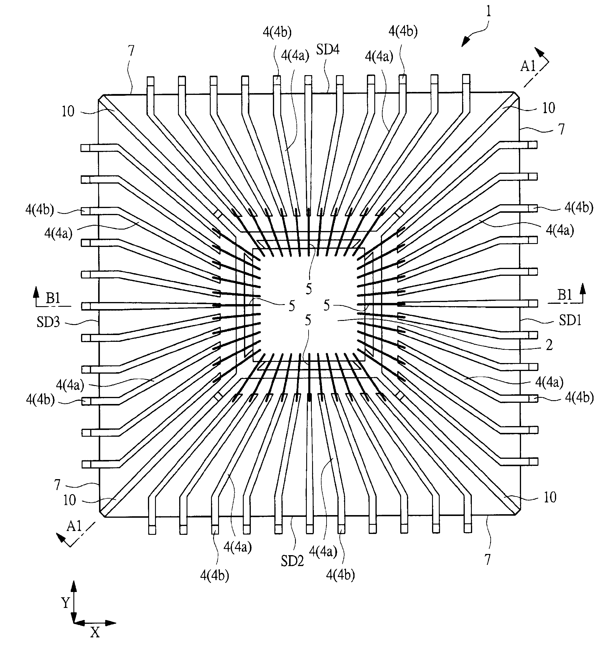
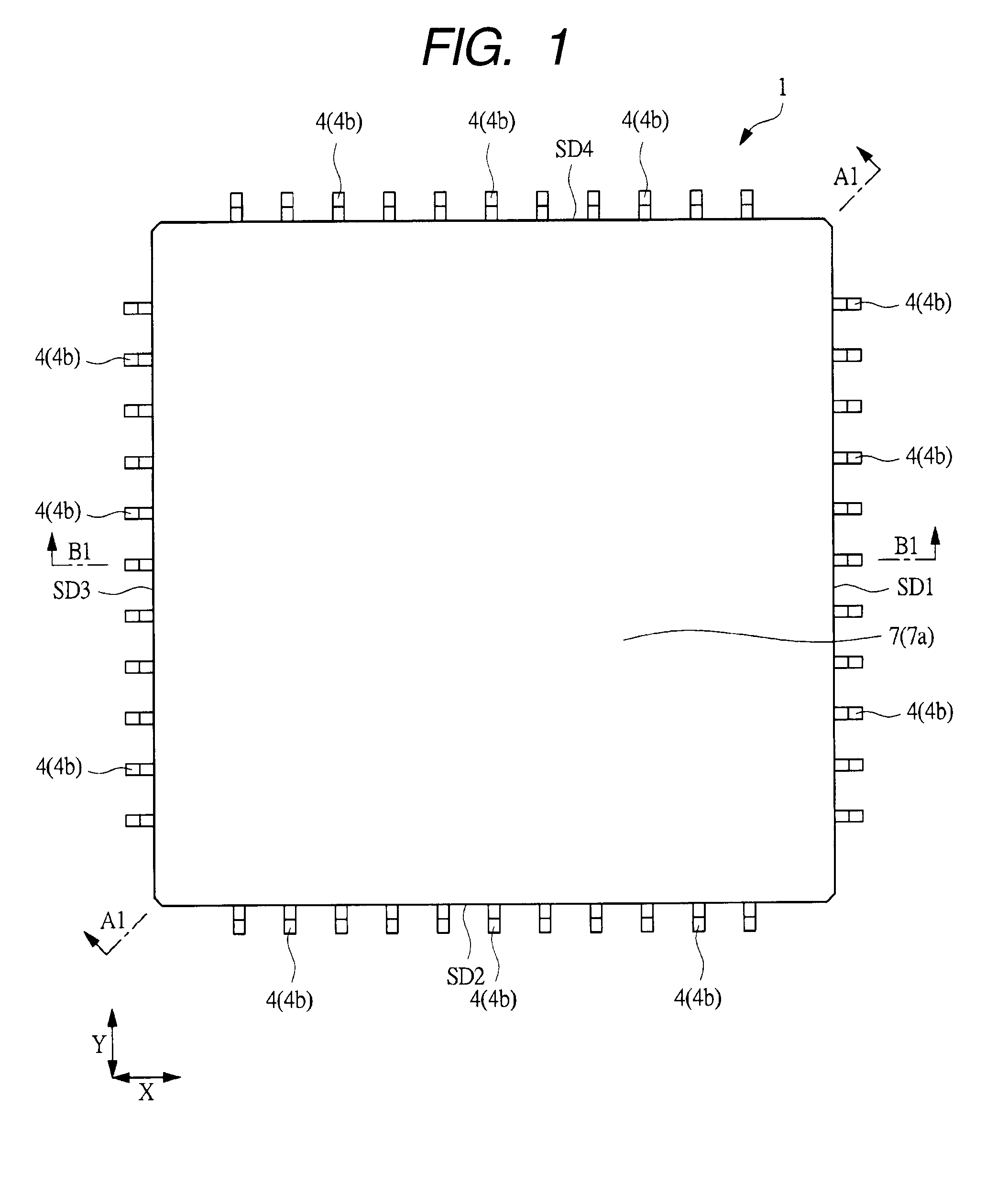
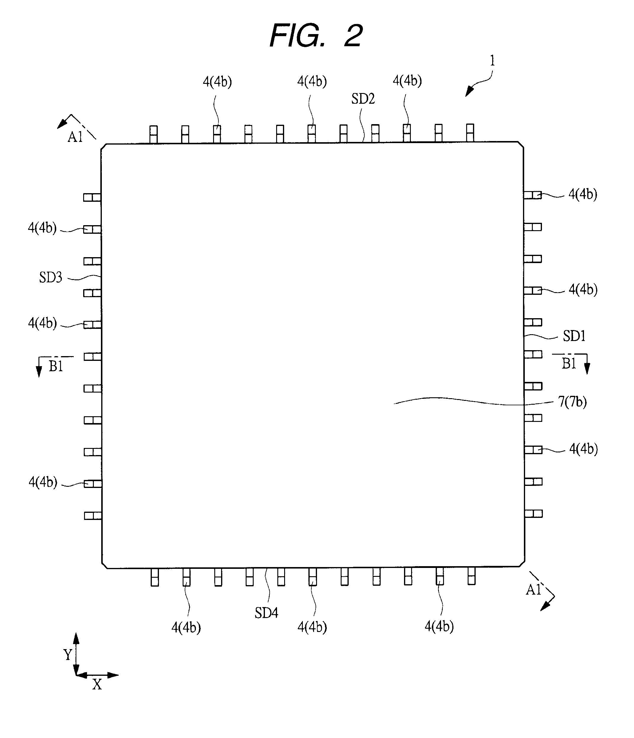
[0099]FIG. 1 is a top view (plan view) of a semiconductor device 1, which is an embodiment of the present invention, FIG. 2 is a bottom view (back view) of the semiconductor device 1, and FIG. 3 is a plan perspective view (top view) of the semiconductor device 1 when a sealing resin part 7 is viewed perspectively. FIG. 4 is a partially enlarged view (partially enlarged plan perspective view) of FIG. 3, showing an enlarged view of the part in the vicinity of the center (a semiconductor chip 2 and a region in the vicinity thereof) in FIG. 3. FIG. 5 is a plan perspective view (partially enlarged plan perspective view) of the semiconductor device 1 when the semiconductor chip 2 and a bonding wire 5 are removed (when viewed perspectively). For easier understanding, the position at which the semiconductor chip 2 is mounted (arranged) is shown by a dotted line in FIG. 5. FIG. ...

second embodiment

[0175]FIG. 18 is a plan perspective view (top view) of semiconductor device 1a in the present embodiment, showing a plan perspective view of the semiconductor device 1a when the sealing resin part 7 is viewed perspectively. FIG. 19 is a partially enlarged view (partially enlarged plan perspective view) of FIG. 18, showing an enlarged view of the part in the vicinity of the center part in FIG. 19 (the semiconductor chip 2 and the region in the vicinity thereof). FIG. 20 is a plan perspective view (partially enlarged plan perspective view) of the semiconductor device 1a when the semiconductor chip 2 and the bonding wire 5 are removed (viewed perspectively) in FIG. 19. FIG. 18, FIG. 19, and FIG. 20 correspond to FIG. 3, FIG. 4, and FIG. 5 in the first embodiment, respectively. As in FIG. 5, in FIG. 20, the position where the semiconductor chip 2 is mounted (arranged) is shown by a dotted line for easier understanding. FIG. 21 to FIG. 23 are each a section view (side section view) of th...

third embodiment

[0194]FIG. 27 is a plan perspective view of essential parts of a semiconductor device of the present invention, corresponding to FIG. 20 in the above-mentioned second embodiment. The present embodiment corresponds to a modified example of the second embodiment. As in FIG. 20, in FIG. 27 also, a plan perspective view of essential parts of a semiconductor device is shown when the sealing resin part 7 is viewed perspectively and further, the semiconductor chip 2 and the bonding wire 5 are removed (viewed perspectively), and for easier understanding, the position where the semiconductor chip 2 is mounted (arranged) is shown by a dotted line.

[0195]In the first and second embodiments described above, the plane figure of the die pad 3 is a circle having a diameter greater than the width (width in the direction perpendicular to the direction in which the member 9 extends from the die pad 3 toward the heat dissipating plate 6) W1 of the member 9. In contrast to that, in the present embodimen...


PUM


Abstract

To improve the heat dissipation characteristics of a semiconductor device.
The semiconductor device has a die pad, a heat dissipating plate in the form of a frame arranged between the die pad and a plurality of leads so as to surround the die pad, a plurality of members that connect the die pad and the inner edge of the heat dissipating plate, and a suspension lead linked to the outer extension of the heat dissipating plate, wherein a semiconductor chip the outer shape of which is larger than the die pad is mounted over the die pad and the members. The top surface of the die pad and the top surface of the members at the part in opposition to the back surface of the semiconductor chip are bonded to the back surface of the semiconductor chip in their entire surfaces with a silver paste. Heat in the semiconductor chip is conducted from the back surface of the semiconductor chip to the heat dissipating plate via the silver paste, the die pad, and the member, and dissipated to the outside of the semiconductor device therefrom via the lead.

Description

CROSS-REFERENCE TO RELATED APPLICATION[0001]The disclosure of Japanese Patent Application No. 2009-86427 filed on Mar. 31, 2009 including the specification, drawings and abstract is incorporated herein by reference in its entirety.BACKGROUND OF THE INVENTION[0002]The present invention relates to a semiconductor device and a method of manufacturing the same, in particular, to technology which is effective when applied to a resin-sealed semiconductor package and a method of manufacturing the same.[0003]A QFP semiconductor device is manufactured by mounting a semiconductor chip over a chip mounting part of a lead frame, coupling a plurality of leads of the lead frame and a plurality of electrodes of the semiconductor chip with a bonding wire, forming a sealing resin part that seals the chip mounting part, the semiconductor chip, the bonding wire, and the inner lead part of the leads, cutting the lead from the lead frame, and bending the outer lead part of the lead.[0004]Japanese Patent...

Claims


Application Information

Patent Timeline
Patent Type & Authority Applications(United States)
IPC IPC(8): H01L23/495H01L21/60
CPCH01L23/3107H01L23/49503H01L24/29H01L2224/32014H01L2224/32057H01L2224/32245H01L2224/48091H01L2224/48108H01L2224/48247H01L2224/49171H01L2224/73265H01L2224/83192H01L2224/83385H01L2224/92247H01L2924/01005H01L2924/01029H01L2924/01046H01L2924/01047H01L2924/01052H01L2924/01057H01L2924/01074H01L2924/01078H01L2924/01079H01L2924/01082H01L2924/14H01L24/48H01L2224/29H01L2224/2919H01L2924/01006H01L2924/01019H01L2924/01033H01L2924/014H01L2924/0665H01L2224/29101H01L24/49H01L24/75H01L24/83H01L2224/45144H01L2224/45147H01L2224/2929H01L2224/29339H01L2924/00013H01L2924/1306H01L2924/00014H01L2924/00012H01L2924/00H01L2924/3512H01L2224/29099H01L2224/29199H01L2224/29299H01L24/45H01L24/73H01L2224/05554H01L2224/32055H01L2924/181H01L2224/05599
Inventor ARITA, JUNICHIHANAWA, KAZUKONISHIMURA, MAKOTO
Owner RENESAS ELECTRONICS CORP
Why Eureka
Try Eureka