Semiconductor integrated circuit device

Active Publication Date: 2010-09-30
KIOXIA CORP
View PDF1 Cites 18 Cited by
  • Summary
  • Abstract
  • Description
  • Claims
  • Application Information

AI Technical Summary

Benefits of technology

[0009]A semiconductor integrated circuit device according to an aspect of the present invention includes an amplification portion having a first transistor configured to inversely amplify an input signal inputted to a gate and output the inversely amplified input signal from a drain, a cascode current source composed of the first transistor, a second transistor having a drain connected to a source of the first transistor and a source connected to a reference potential point to supply a bias current to the first transistor, a third transistor having a gate connected to the gate of the first transistor in a DC manner, a fourth transistor having a gate connected to a gate of the second transistor, and a current source, and configured to control the bias current based on a current flowing into the current source, and a resistive element configured to disconnect the drain of the first transistor and the gates of the first and third transistors in an AC manner and connect the drain of the

Problems solved by technology

For the reason, the invention of Document 1 is disadvantageous, e.g., in that the inverting amplifier is susceptible to common mode noise, and output amplitude may become small or oscillation may occur due to in-phase components.
However, in a transistor, an output impedance decreases, and a drain current increases with a rise in output voltage, due to channel length modulation effect caused by miniaturization.
A transistor thus cannot constitute an ideal current source.

Method used


Image

  • Semiconductor integrated circuit device
  • Semiconductor integrated circuit device
  • Semiconductor integrated circuit device

Examples


first embodiment

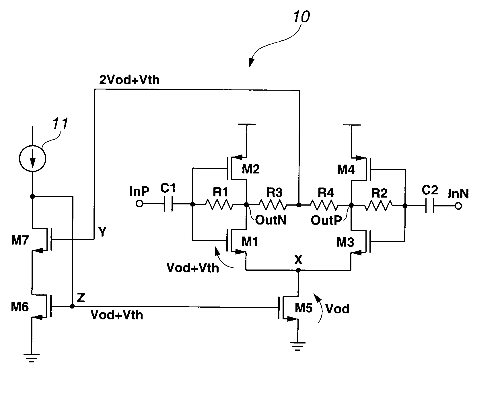
[0020]FIG. 1 is a circuit diagram showing a semiconductor integrated circuit according to a first embodiment of the present invention.

[0021]The semiconductor integrated circuit in FIG. 1 constitutes an inverting amplifier. Use of a cascode current source as a current source of an inverting amplifier or the like for an improvement in characteristics is contemplated. A cascode current source can be composed of two transistors cascoded between a reference potential point and a common source of a pair of transistors with a differential configuration constituting an inverting amplifier. A current source with the configuration is higher in output impedance than a current source using one transistor by a magnitude corresponding to an additional cascoded transistor. A cascode current source thus has an advantage of having improved current source characteristics.

[0022]Design of a DC characteristic of an inverting amplifier requires consideration of a minimum acceptable voltage (overdrive vol...

second embodiment

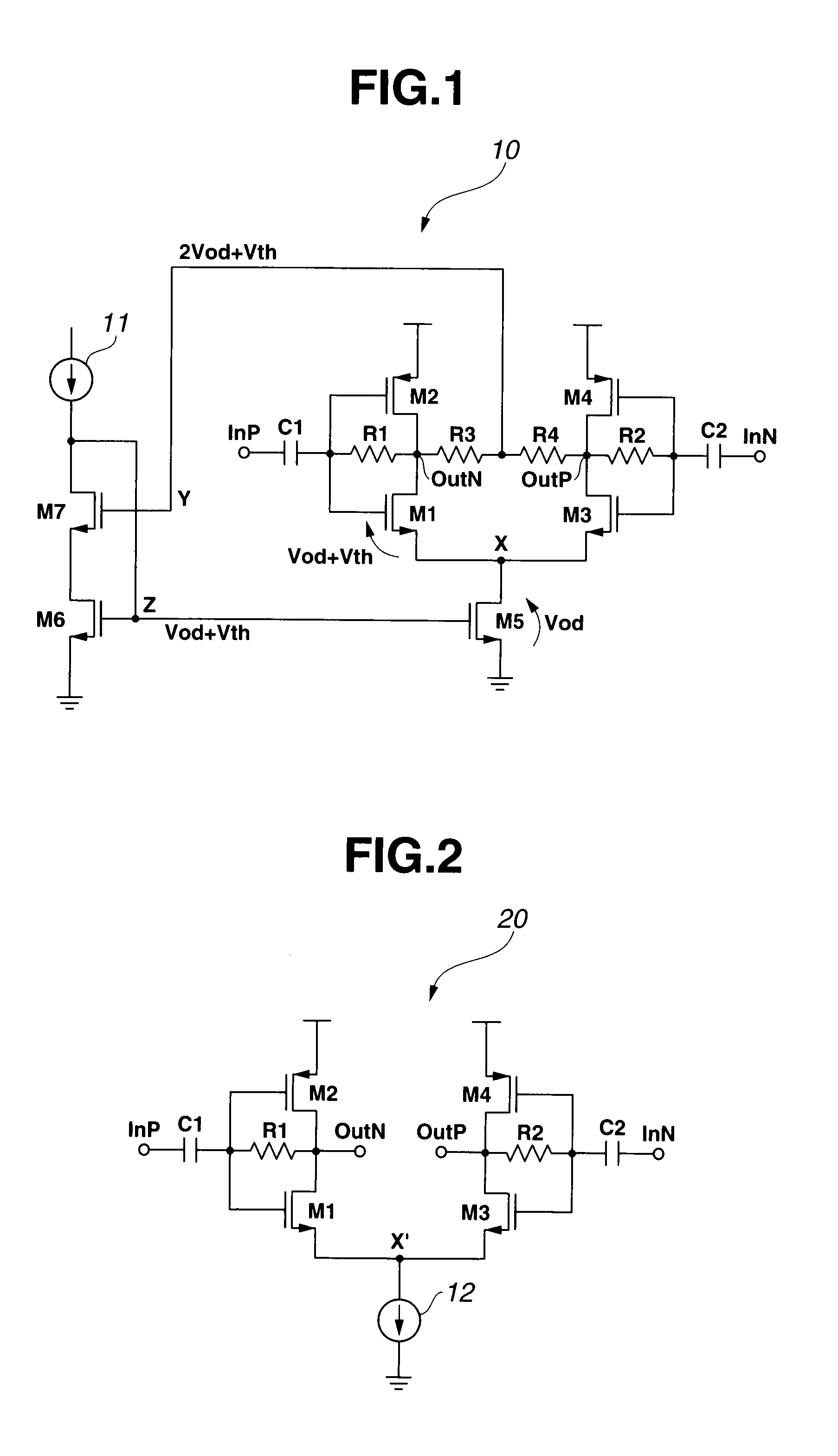
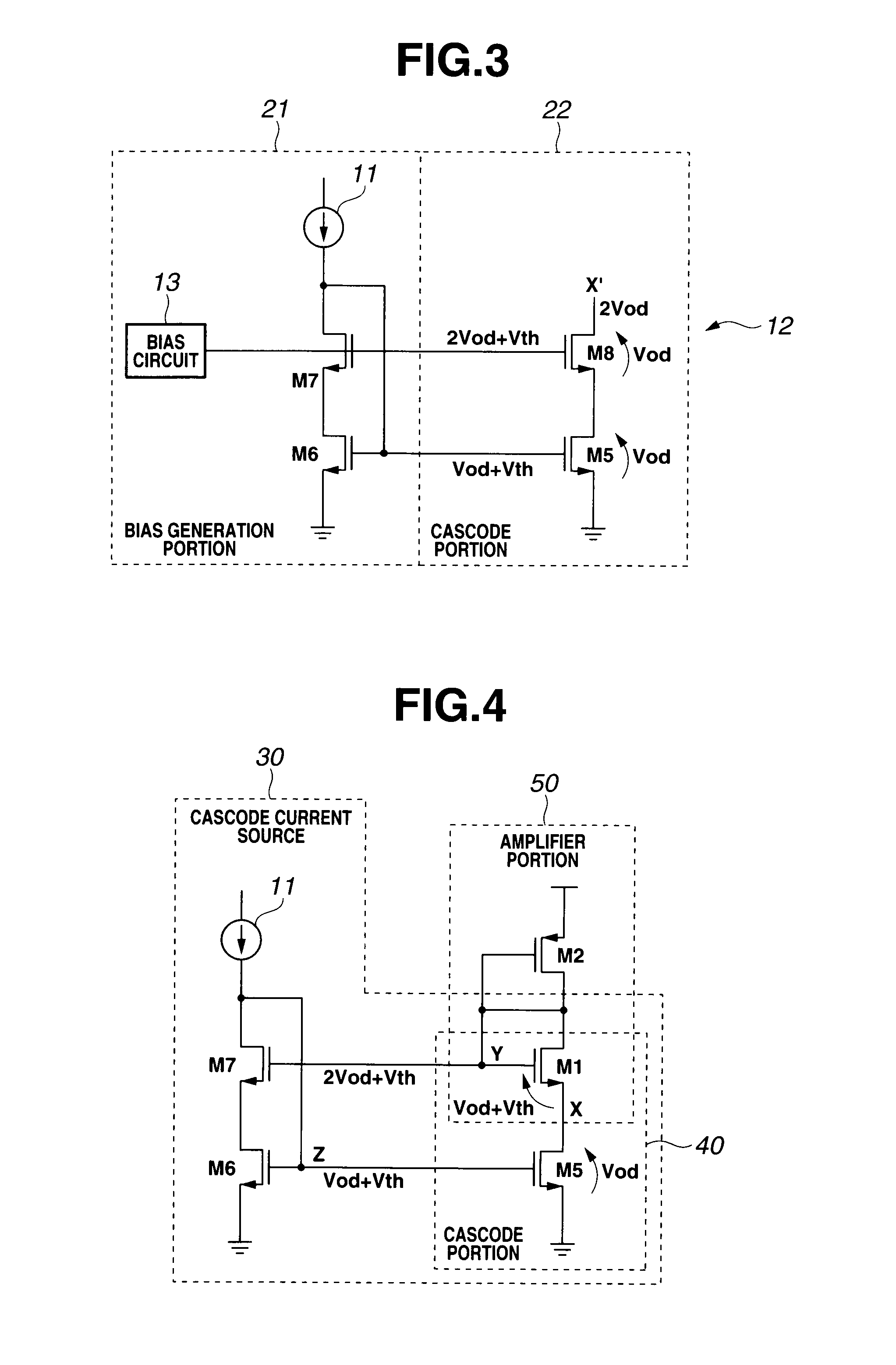
[0052]FIG. 7 is a circuit diagram showing a second embodiment of the present invention. Same components in FIG. 7 as in FIGS. 1 and 2 are denoted by same reference numerals, and a description of the components will be omitted.

[0053]In the first embodiment, the resistors R3 and R4 are provided between the output terminals OutN and OutP and the gate of the transistor M7 to connect between the output terminals OutN and OutP and the gate of the transistor and M7 in a DC manner, as shown in FIG. 1. However, since a parasitic capacitance (not shown) is produced for each of the resistors R3 and R4, characteristics of the inverting amplifier may deteriorate.

[0054]For the reason, in the present embodiment, a replica circuit configured to determine a DC characteristic of an inverting amplifier is provided. The configuration makes it possible to omit the resistors R3 and R4 and prevent deterioration of characteristics. An inverting amplifier 60 shown in FIG. 7 adopts a cascode current source r...


PUM


Abstract

A semiconductor integrated circuit device constituting an inverting amplifier employs a cascode current source as a current source. In the semiconductor integrated circuit device, a high-potential-side transistor of the cascode current source and a low-potential-side transistor constituting an amplification portion are shared. The configuration can not only make an output impedance of the cascode current source high and improve current source characteristics but also make a minimum potential at a minimum potential point of the amplification portion low and ensure a sufficient power supply voltage margin.

Description

CROSS-REFERENCE TO RELATED APPLICATION[0001]This application is based upon and claims the benefit of priority from the prior Japanese Patent Application No. 2009-86572 filed in Japan on Mar. 31, 2009; the entire contents of which are incorporated herein by reference.BACKGROUND OF THE INVENTION[0002]1. Field of the Invention[0003]The present invention relates to a semiconductor integrated circuit device suitable for an inverting amplifier.[0004]2. Description of Related Art[0005]An inverting amplifier is often used in a conventional analog circuit. For example, in a radio transceiver, inverting amplifiers are used in circuit blocks such as a local oscillation buffer circuit and a current-voltage conversion circuit, and frequency of use of inverting amplifiers is high.[0006]As an example of such an inverting amplifier, a CMOS inverting amplifier configured to perform stable amplification at low voltage is disclosed in Japanese Patent Application Laid-Open Publication No. 2006-60606 (h...

Claims


Application Information

Patent Timeline
IPC IPC(8): H03F3/16
CPCH03F3/3028H03F3/45179H03F3/45183H03F3/505H03F2200/453H03F2203/45236H03F2203/45702H03F2203/45394H03F2203/45508H03F2203/45528H03F2203/45544H03F2203/45696H03F2203/45698H03F2203/45244
Inventor DEGUCHI, JUNKOBAYASHI, NAOKI
Owner KIOXIA CORP
Why Eureka
Try Eureka