
High-Mobility Multiple-Gate Transistor with Improved On-to-Off Current Ratio

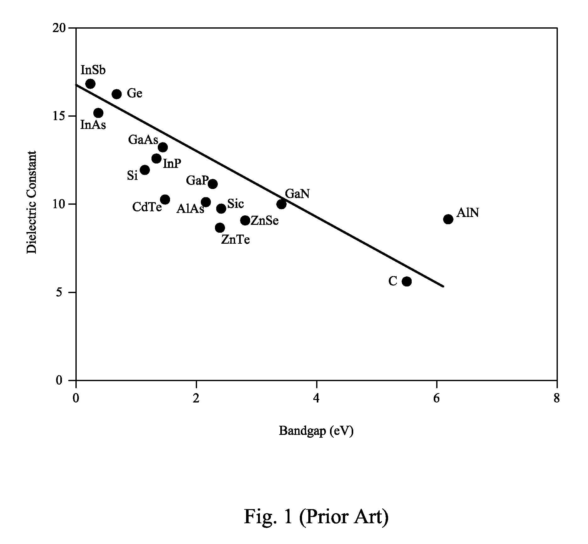
a technology of metal oxides and transistors, applied in the field of integrated circuit devices, can solve the problems of no longer being able to provide convenience from silicon oxides, not being suitable for gate dielectric formation, and germanium oxide, so as to improve the performance of mos transistors, reduce leakage currents, and improve drive currents

Active Publication Date: 2010-10-07
TAIWAN SEMICON MFG CO LTD
View PDF71 Cites 103 Cited by
  • Summary
  • Abstract
  • Description
  • Claims
  • Application Information

AI Technical Summary

Benefits of technology

[0012]The advantageous features of the present invention include improved performance in MOS transistors including improved drive currents, reduced leakage currents, and high on-to-off current ratios.

Problems solved by technology

The oxide of germanium, on the other hand, is soluble in water, and hence is not suitable for the formation of gate dielectrics.
With the use of high-k dielectric materials in the gate dielectrics of MOS transistors, however, the convenience provided by the silicon oxide is no longer a big advantage, and hence germanium is reexamined for use in integrated circuits.
A challenge faced by the semiconductor industry is that although the MOS transistors formed on germanium and III-V compound semiconductors have high drive currents, the leakage currents of these MOS transistors are also high.
Therefore, the respective MOS transistors suffer from band-to-band leakage currents between their gates and source / drain regions.
As a result, the on / off current ratios (Ion / Ioff) of these MOS transistors are relatively low.

Method used


Image

  • High-Mobility Multiple-Gate Transistor with Improved On-to-Off Current Ratio
  • High-Mobility Multiple-Gate Transistor with Improved On-to-Off Current Ratio
  • High-Mobility Multiple-Gate Transistor with Improved On-to-Off Current Ratio

Examples


Embodiment Construction

[0026]The making and using of the embodiments of the present invention are discussed in detail below. It should be appreciated, however, that the embodiments provide many applicable inventive concepts that can be embodied in a wide variety of specific contexts. The specific embodiments discussed are merely illustrative of specific ways to make and use the invention, and do not limit the scope of the invention.

[0027]Novel fin field-effect transistors (FinFETs) and the methods of forming the same are presented. The intermediate stages of manufacturing embodiments of the present invention are illustrated. The variations and the operation of the embodiments are discussed. Throughout the various views and illustrative embodiments of the present invention, like reference numbers are used to designate like elements.

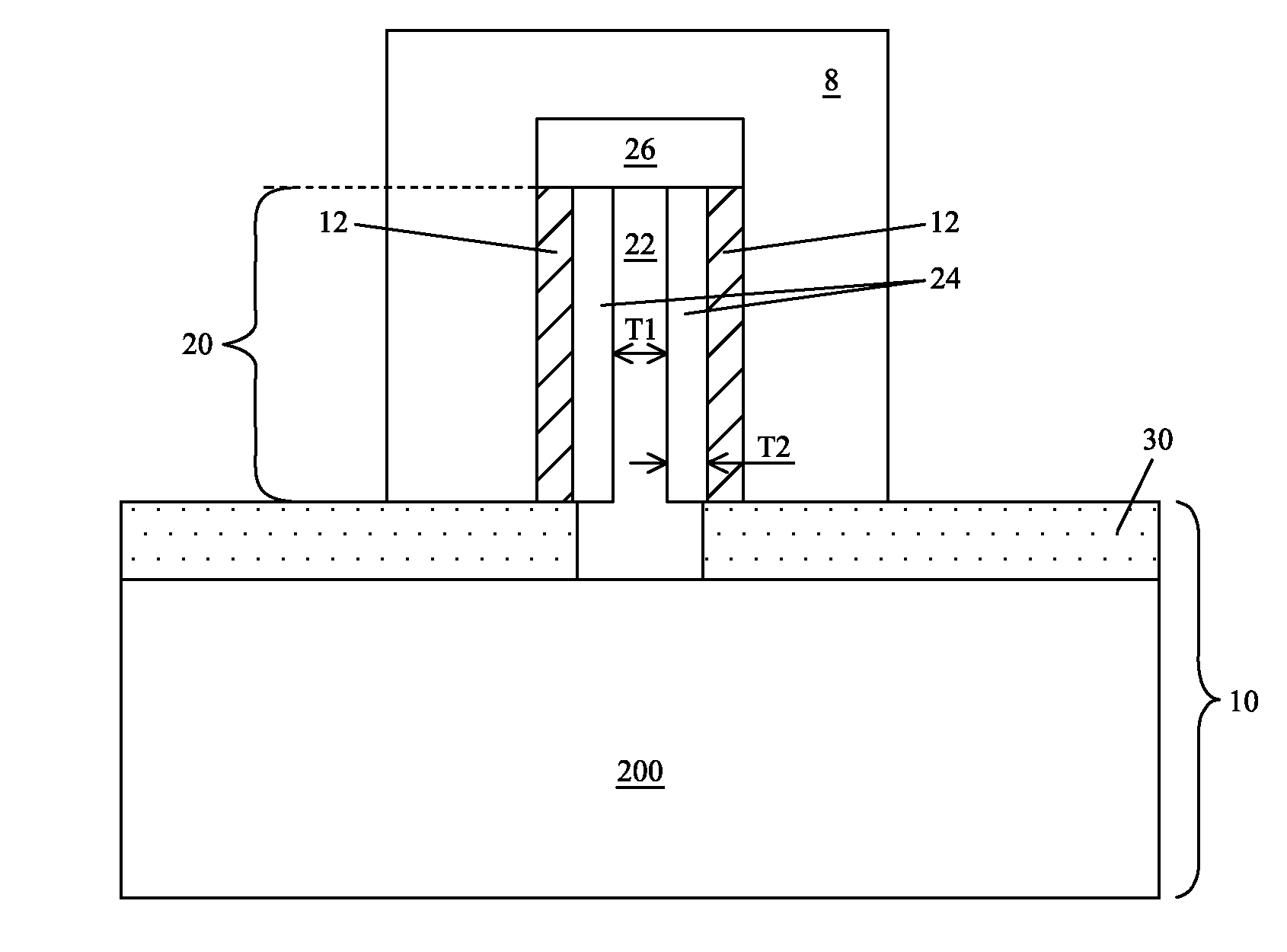
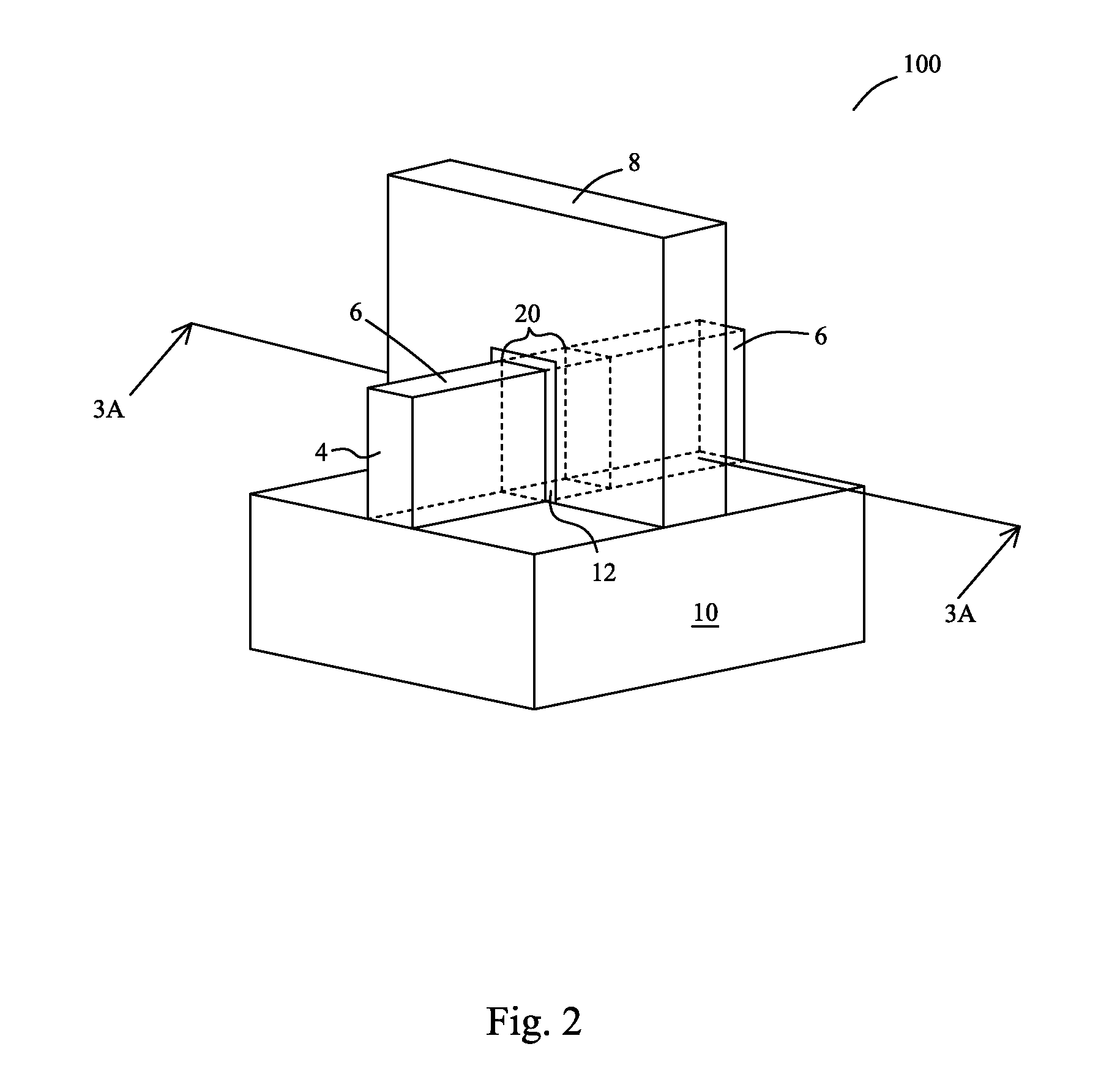
[0028]FIG. 2 illustrates a perspective view of FinFET 100 (which may be an n-type FinFET) formed on base material 10. Base material 10 may be formed of a dielectric material, fo...


PUM


Abstract

A multi-gate transistor includes a semiconductor fin over a substrate. The semiconductor fin includes a central fin formed of a first semiconductor material; and a semiconductor layer having a first portion and a second portion on opposite sidewalls of the central fin. The semiconductor layer includes a second semiconductor material different from the first semiconductor material. The multi-gate transistor further includes a gate electrode wrapping around sidewalls of the semiconductor fin; and a source region and a drain region on opposite ends of the semiconductor fin. Each of the central fin and the semiconductor layer extends from the source region to the drain region.

Description

[0001]This application claims the benefit of U.S. Provisional Application No. 61 / 165,803 filed on Apr. 1, 2009, entitled “High-Mobility Multiple-Gate Transistor with Improved On-to-Off Current Ratio,” which application is hereby incorporated herein by reference.TECHNICAL FIELD[0002]This invention relates generally to integrated circuit devices, and more particularly to metal-oxide-semiconductor (MOS) transistors and methods for forming the same.BACKGROUND[0003]The speeds of metal-oxide-semiconductor (MOS) transistors are closely related to the drive currents of the MOS transistors, which drive currents are further closely related to the mobility of charges. For example, NMOS transistors have high drive currents when the electron mobility in their channel regions is high, while PMOS transistors have high drive currents when the hole mobility in their channel regions is high.[0004]Germanium is a commonly known semiconductor material. The electron mobility and hole mobility of germaniu...

Claims


Application Information

Patent Timeline
Patent Type & Authority Applications(United States)
IPC IPC(8): H01L29/66H01L29/78
CPCH01L29/66818H01L29/785H01L29/812H01L29/66431H01L29/66484H01L29/66795H01L29/7831H01L29/42312H01L29/1054H01L29/122H01L29/8124
Inventor KO, CHIH-HSINWANN, CLEMENT HSINGJEN
Owner TAIWAN SEMICON MFG CO LTD
Features
  • Generate Ideas
  • Intellectual Property
  • Life Sciences
  • Materials
  • Tech Scout
  • Unparalleled Data Quality
  • Higher Quality Content
  • 60% Fewer Hallucinations
Learn More