Methods of Patterning Substrates Using Microcontact Printed Polymer Resists and Articles Prepared Therefrom

a technology of printed polymer resist and patterning substrate, which is applied in the field of method of patterning substrate, can solve the problems of difficult and/or costly patterning on very large and/or non-rigid surfaces such as textiles, paper, plastics, etc., and achieve the effects of cost-effective, efficient and reproducibl

Inactive Publication Date: 2010-10-07
NANO TERRA INC +1
View PDF3 Cites 13 Cited by
  • Summary
  • Abstract
  • Description
  • Claims
  • Application Information

AI Technical Summary

Benefits of technology

[0009]The present invention is directed to patterning substrates using contact-printing techniques that employ a “resist composition” comprising a thermoelastic polymer. The resist compositions are capable of forming a substantially uniform film on a stamp that is substantially free from cracks. A stamp coated with the resist composition can be contacted with a substrate to provide a pattern of the resist composition thereon, wherein the pattern has a predetermined lateral dimension defined by a pattern in the stamp surface. The resist compositions are resistant to many classes of etchants and other reactive compositions suitable for reacting with substrates of interest. In some embodiments, a thermoelastic polymers present in the resist composition is readily soluble in a variety of solvents, thereby permitting facile removal of a resist pattern from a substrate after exposure of the substrate to a reactive composition. Features formed by the methods of the present invention have lateral dimensions less than 50 μm, and permit all varieties of substrates to be patterned in a cost-effective, efficient, and reproducible manner.

Problems solved by technology

Such photolithographic patterning methods, while versatile in the variety of surface features and compositions that can be patterned, are also costly and require specialized equipment and specialized resist compositions suitable for interacting with UV light.
Moreover, patterning very large and / or non-rigid surfaces such as, for example, textiles, paper, plastics, and the like using photolithographic resists can be difficult and / or costly.
However, the low chemical resistance of most materials that can be patterned by microcontact printing processes has in some cases limited the applications of microcontact printing.

Method used


Image

  • Methods of Patterning Substrates Using Microcontact Printed Polymer Resists and Articles Prepared Therefrom
  • Methods of Patterning Substrates Using Microcontact Printed Polymer Resists and Articles Prepared Therefrom
  • Methods of Patterning Substrates Using Microcontact Printed Polymer Resists and Articles Prepared Therefrom

Examples


example 1

[0212]A 200 mm by 200 mm square-shaped stamp comprising a flexible material (polydimethylsiloxane, “PDMS”) having a desired topography was prepared from a master using methods previously described elsewhere. See, e.g., U.S. Pat. Nos. 5,512,131 and 5,900,160, which are incorporated herein by reference in their entirety. The stamp was spin-coated with a thin layer of a resist composition comprising a thermoelastic polymer (styrene-(ethylene-butylene) triblock copolymer grafted with maleic anhydride, “SEBMA”) in a solvent (toluene), 1.5% SEBMA, by weight. The thermoelastic polymer-coated stamp was then contacted for 60 seconds with a composite substrate of a 270 nm thick indium-tin-oxide (“ITO”) layer coated on a glass support. The temperature of the substrate was maintained at 130° C. during the contacting. The stamp was then removed from the substrate, and the substrate was annealed approximately 60 s at 130° C. The resulting thermoelastic polymer pattern on the substrate had a thick...

example 2

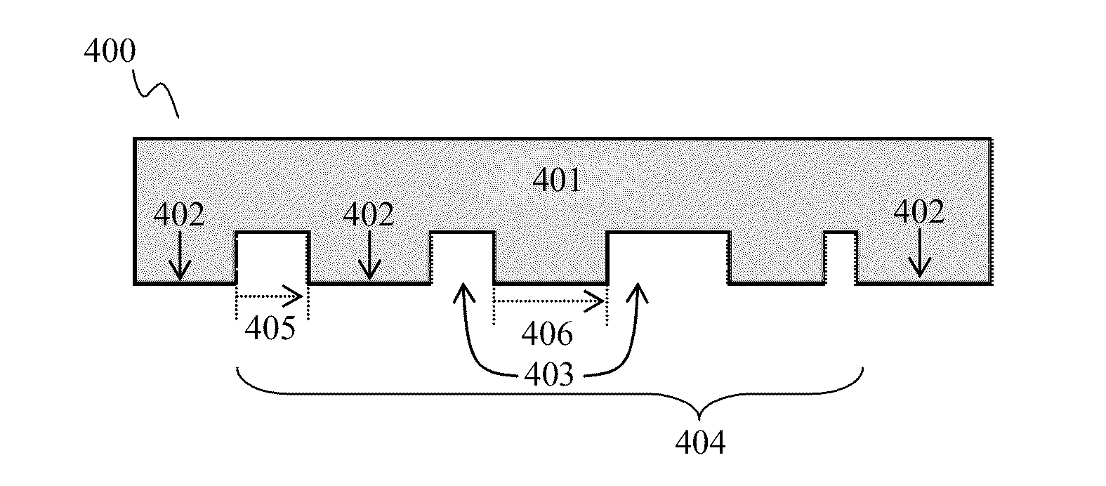
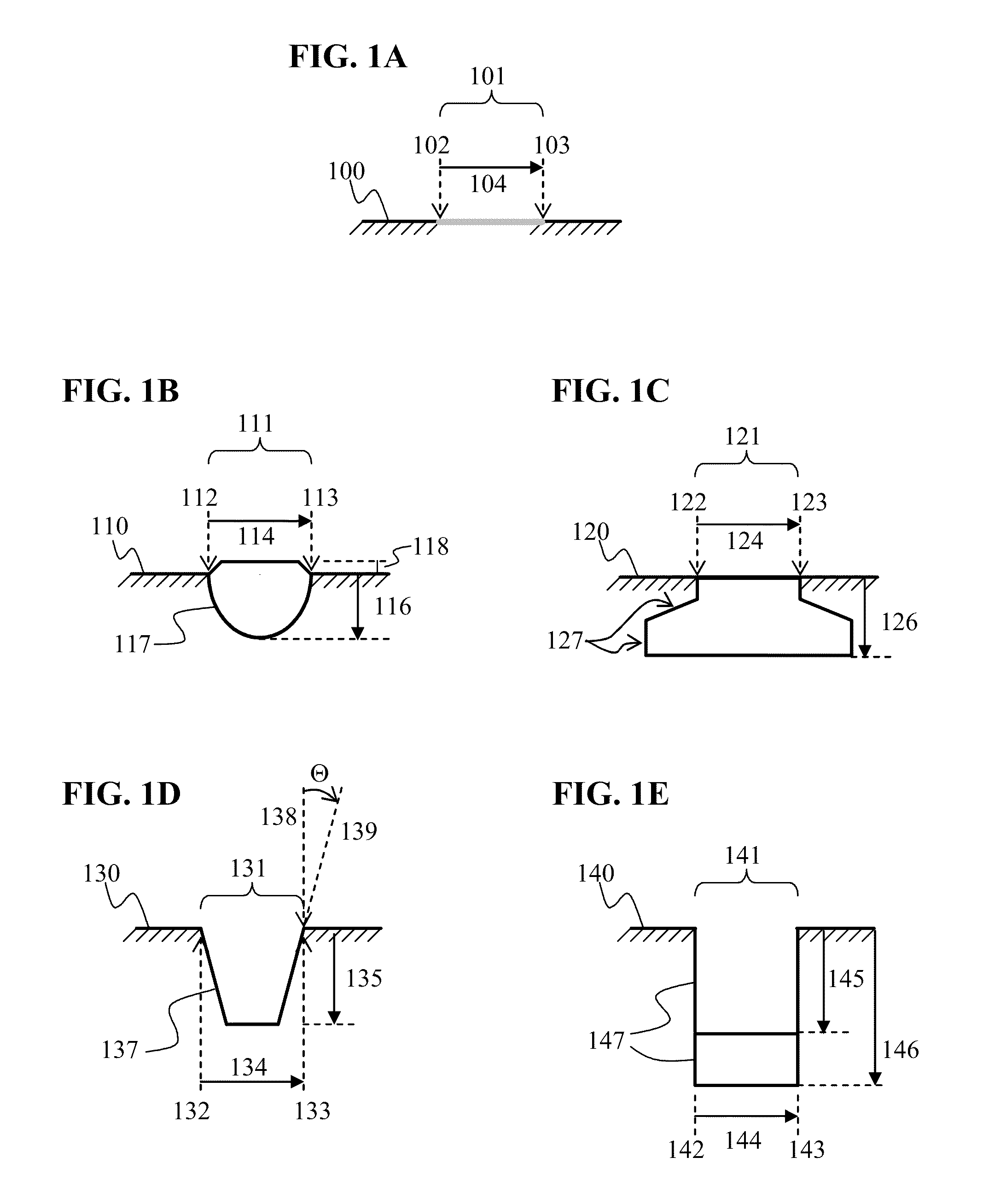
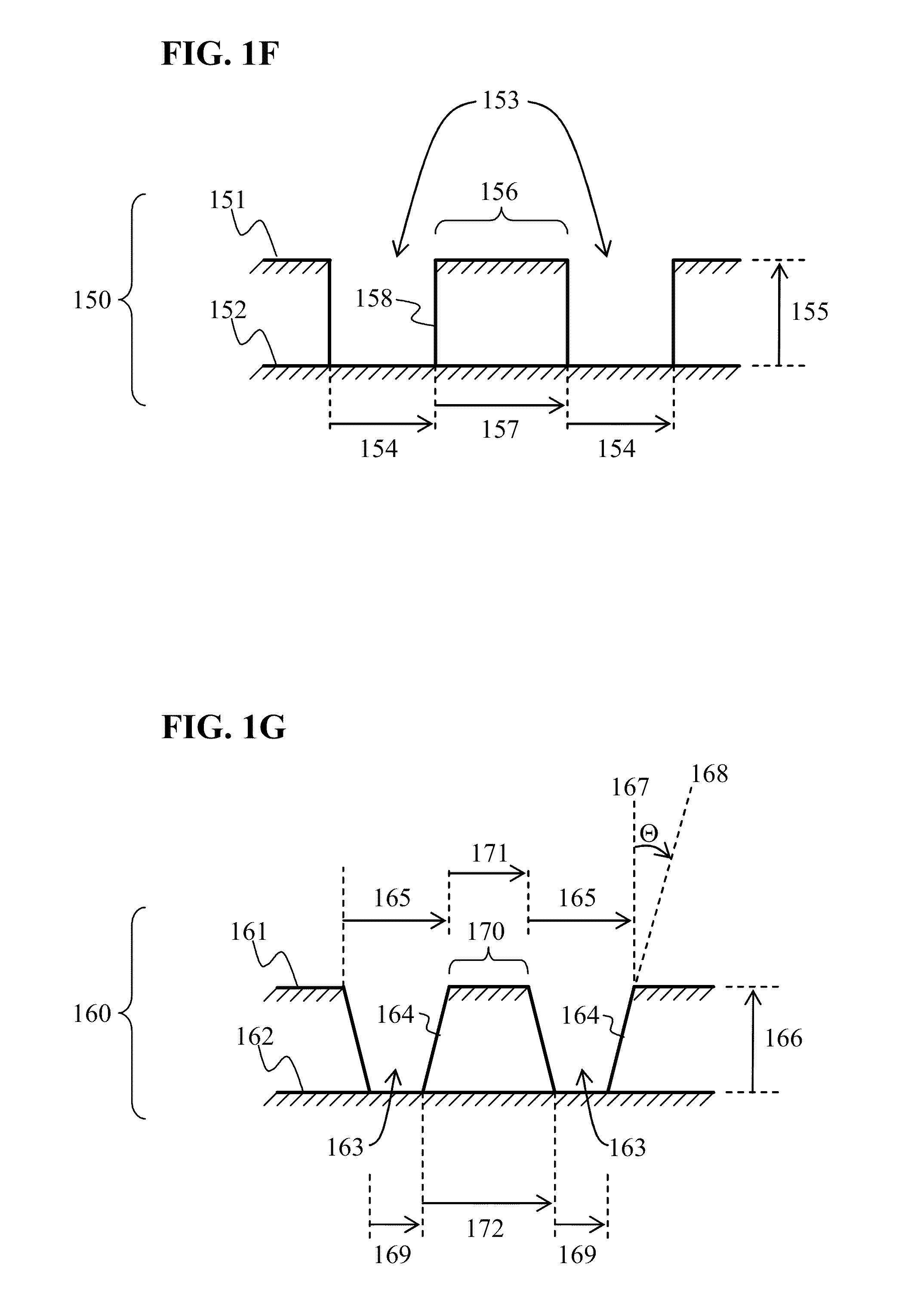
[0220]The patterned substrates prepared in Example 1 were quantitatively analyzed to determine the type and number of defects as well as the average feature size of the patterns formed. The results are summarized in Table 1. The top-lateral dimension (“TLD”) refers to the lateral dimension of the subtractive non-penetrating features as measured on the surface of the substrate (i.e., lateral dimension 165 in FIG. 1G). The first lateral dimension measured at the base of the feature (“BLD1”) refers to the lateral dimension of the subtractive non-penetrating feature at the base of the feature (i.e., lateral dimension 169 in FIG. 1G). The difference between these lateral dimension, Δ, is related to the sidewall angle. The features had a height of 270 nm.

TABLE 1Defect rate and lateral dimensions of subtractivenon-penetrating features formed in a composite substrate(ITO on glass), as described in Example 1.Avg. Per100 FeaturesSample 1Sample 2Sample 3AverageBridging0000DefectsPairing0000Def...

example 3

[0222]The patterning method described in Example 1 was used to pattern a 200 mm×200 mm square glass substrate having a 270 nm ITO coating thereon. The resulting pattern of ITO islands surrounded by subtractive non-penetrating features is shown in FIG. 15. Referring to FIG. 15, a top-view microscope image, 1500, of a patterned substrate from which a portion of an ITO coating has been removed is provided. The patterned substrate includes areas comprising rectilinear-shaped ITO islands, 1501, as well as triangular shaped ITO-islands, 1502, on a glass substrate.


PUM

PropertyMeasurementUnit
Young's Modulusaaaaaaaaaa
molecular weightaaaaaaaaaa
boiling pointaaaaaaaaaa

Abstract

The present invention is directed to methods for patterning substrates using contact printing to form patterns comprising a polymer, using the patterns formed therefrom as resists, and process products formed by the process.

Description

CROSS-REFERENCE TO RELATED APPLICATIONS[0001]This application claims the benefit of the filing date of U.S. Appl. No. 61 / 165,755, filed Apr. 1, 2009, which is incorporated herein by reference in its entirety.BACKGROUND OF THE INVENTION[0002]1. Field of the Invention[0003]The present invention is directed to methods for patterning substrates using contact printing processes that employ a stamp to apply a resist composition comprising a thermoelastic polymer to a substrate, as well as resists and compositions comprising the resists.[0004]2. Background[0005]Resists are frequently used in the electronics industry to selectively pattern substrates by protecting predetermined areas of a substrate during etching, doping, and deposition processes and the like. Resists typically comprise a polymer and / or polymer precursor along with a solvent carrier, and are deposited by spin-coating or some other blanket deposition process. The deposited resist can then be patterned using, e.g., photolitho...

Claims


Application Information

Patent Timeline
Patent Type & Authority Applications(United States)
IPC IPC(8): B29C59/02C08L41/00C08L37/00C08L39/00C08L55/00C08L25/08C08L33/12
CPCB82Y10/00B82Y40/00G03F7/0002C09D153/025C09D153/02C09D151/003C08L35/06C08L33/12C08L33/20C08L2666/02
Inventor AGARWAL, SANDIPMAYERS, BRIAN T.MCLELLAN, JOSEPH M.KUGLER, RALFKURSAWE, MONIKA
Owner NANO TERRA INC
Why Eureka
Try Eureka